SLOS856B June 2013 – May 2017 OPA2322-Q1 , OPA322-Q1 , OPA4322-Q1
PRODUCTION DATA.
- 1 Features
- 2 Applications
- 3 Description
- 4 Revision History
- 5 Pin Configuration and Functions
- 6 Specifications
- 7 Typical Characteristics
- 8 Detailed Description
- 9 Application and Implementation
- 10Power Supply Recommendations
- 11Layout
- 12Device and Documentation Support
- 13Mechanical, Packaging, and Orderable Information
1 Features
- Qualified for Automotive Applications
- AEC-Q100 Qualified With the Following Results:
- Device Temperature Grade 1: –40°C to +125°C Ambient Operating Temperature Range
- Device HBM ESD Classification Level H3A
- Device CDM ESD Classification Level C5
- Gain Bandwidth: 20 MHz
- Low Noise: 8.5 nV√Hz at 1 kHz
- Slew Rate: 10 V/μs
- Low THD+N: 0.0005%
- Rail-to-Rail I/O
- Offset Voltage: 2 mV (Maximum)
- Supply Voltage: 1.8 V to 5.5 V
- Supply Current:
- Unity-Gain Stable
- Small Packages:
2 Applications
- Automotive
- Sensor Signal Conditioning
- Consumer Audio
- Multi-Pole Active Filters
- Control-Loop Amplifiers
- Communications
- Security
- Scanners
3 Description
The OPAx322-Q1 series consists of single-, dual-, and quad-channel CMOS operational amplifiers featuring low noise and rail-to-rail inputs and outputs optimized for low-power, single-supply applications. Specified over a wide supply range from 1.8 V to 5.5 V, the low quiescent current of only 1.5 mA per channel makes these devices well-suited for power-sensitive applications.
The combination of very-low noise (8.5 nV√Hz at 1 kHz), high-gain bandwidth (20 MHz), and fast slew rate (10 V/μs) make the OPAx322-Q1 family ideal for a wide range of applications, including signal conditioning and sensor amplification requiring high gains. Featuring low THD+N, the OPAx322-Q1 family is also excellent for consumer audio applications, particularly for single-supply systems.
The OPA322-Q1 (single version) is available in 5-pin SOT-23 package, while the OPA2322-Q1 (dual version) is offered in a 8-pin VSSOP package. The OPA4322-Q1 (quad version) is available in a 14-pin TSSOP package. All versions are specified for operation from –40°C to +125°C.
Device Information(1)
| PART NUMBER | PACKAGE | BODY SIZE (NOM) |
|---|---|---|
| OPA322-Q1 | SOT-23 (5) | 2.90 mm × 1.60 mm |
| OPA2322-Q1 | VSSOP (8) | 3.00 mm × 3.00 mm |
| OPA4322-Q1 | TSSOP (14) | 5.00 mm × 4.40 mm |
- For all available packages, see the orderable addendum at the end of the data sheet.
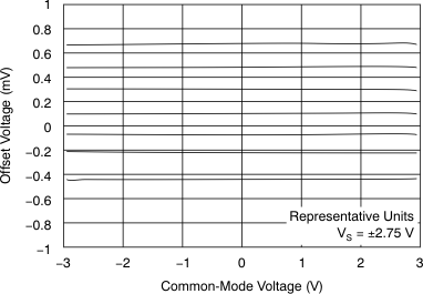
Zero-Crossover Rail-to-Rail Input Stage Eliminates Distortion

4 Revision History
Changes from A Revision (June 2013) to B Revision
- Updated data sheet text to the latest documentation and translation standardsGo
- Deleted "x" device marking and "with shutdown" from document title Go
- Deleted "Shutdown: 0.1 µA/ch" from Features list Go
- Deleted SON package from Features list Go
- Deleted OPA322S-Q1, OPA2322S-Q1, OPA4322S-Q1 devices from data sheet Go
- Changed single-supply current from 1.5 mA/ch to 1.6 mA/ch in Features sectionGo
- Changed quad-supply current from 1.5 ma/ch to 1.4 ma/ch in Features section Go
- Deleted "x" device marking, 6-pin SOT-23, 16-pin TSSOP, 10-pin VSSOP, 8-pin SOIC, 8-pin SON packages and shutdown text from Description section Go
- Deleted OPA322S-Q1, OPA2322S-Q1, and OPA4322S-Q1 devices from Device Information table Go
- Deleted 8-pin SOIC and 8-pin SON packages from Device Information table Go
- Deleted OPA322S-Q1 pinout drawing and pin table information in Pin Configuration and Functions section Go
- Deleted OPA2322-Q1 DRG package pinout drawing in Pin Configuration and Functions sectionGo
- Deleted OPA2322S-Q1 pinout drawing and table information in Pin Configuration and Functions section Go
- Deleted OPA4322S-Q1 pinout drawing and table information in Pin Configuration and Functions section Go
- Updated OPA2322-Q1 pinout tables in Pin Configuration and Functions section Go
- Updated OPA4322-Q1 pinout table in Pin Configuration and Functions section Go
- Deleted Operating Temperature, TA values from Absolute Maximum Ratings tableGo
- Added automotive ESD Ratings table to the Specifications sectionGo
- Added Recommended Operating Conditions table to the Specifications sectionGo
- Deleted OPA322S-Q1 Thermal Information table Go
- Deleted OPA2322S-Q1 D and DRG package Thermal Information valuesGo
- Deleted OPA2322S-Q1 Thermal Information table values Go
- Deleted OPA4322S-Q1 Thermal Information table values Go
- Deleted shutdown information from Electrical Characteristics table Go
- Changed typical input voltage noise value from 2.8 to 4.5 µVPP in Electrical Characteristics tableGo
- Deleted repeating Open-Loop Gain test conditions in Electrical Characteristics table Go
- Deleted Figure 26, Figure 27, Figure 28, and Figure 29 from Typical Characteristics section Go
- Updated x-axis of Figure 2 Go
- Updated x-axis of Figure 5 Go
- Added Detailed Description section and Functional Block DiagramGo
- Added Feature Description section Go
- Deleted shutdown text in Feature Description section Go
- Deleted text regarding the unity-gain stability of the OPAx322-Q1 in 1-nF capacitive loads Capacitive Load and Stability section Go
- Added Device Functional Modes section Go
- Deleted shutdown text in Device Functional Modes section Go
- Changed FilterPro™ link in Application Information section Go
- Updated Figure 35 Go
- Added Power Supply Recommendations section Go
- Added Layout section Go
- Deleted Leadless DFN Package subsection in Layout section Go
- Updated Figure 37 (Layout Example)Go
- Deleted OPA322S-Q1, OPA2322S-Q1, and OPA4322S-Q1 devices from Related Links tableGo
Changes from * Revision (June 2013) to A Revision
- Changed document status to Production Data Go