JAJSFF7F June   2009  – May 2018 OPA2354A-Q1 , OPA354A-Q1 , OPA4354-Q1

PRODUCTION DATA.  

  1. 特長
  2. アプリケーション
  3. 概要
    1.     概略回路図
  4. 改訂履歴
  5. Pin Configuration and Functions
    1.     Pin Functions: OPA354A-Q1
    2.     Pin Functions: OPA2354A-Q1
    3.     Pin Functions: OPA4354-Q1
  6. Specifications
    1. 6.1 Absolute Maximum Ratings
    2. 6.2 ESD Ratings
    3. 6.3 Recommended Operating Conditions
    4. 6.4 Thermal Information: OPA354A-Q1
    5. 6.5 Thermal Information: OPA2354A-Q1
    6. 6.6 Thermal Information: OPA4354A-Q1
    7. 6.7 Electrical Characteristics
    8. 6.8 Typical Characteristics
  7. Detailed Description
    1. 7.1 Overview
    2. 7.2 Functional Block Diagram
    3. 7.3 Feature Description
      1. 7.3.1 Operating Voltage
      2. 7.3.2 Rail-to-Rail Input
      3. 7.3.3 Rail-to-Rail Output
      4. 7.3.4 Output Drive
      5. 7.3.5 Video
      6. 7.3.6 Driving Analog-to-Digital Converters
      7. 7.3.7 Capacitive Load and Stability
      8. 7.3.8 Wideband Transimpedance Amplifier
    4. 7.4 Device Functional Modes
  8. Application and Implementation
    1. 8.1 Application Information
    2. 8.2 Typical Applications
      1. 8.2.1 Transimpedance Amplifier
        1. 8.2.1.1 Design Requirements
        2. 8.2.1.2 Detailed Design Procedure
          1. 8.2.1.2.1 Optimizing The Transimpedance Circuit
        3. 8.2.1.3 Application Curve
      2. 8.2.2 High-Impedance Sensor Interface
      3. 8.2.3 Driving ADCs
      4. 8.2.4 Active Filter
  9. Power Supply Recommendations
    1. 9.1 Power Dissipation
  10. 10Layout
    1. 10.1 Layout Guidelines
    2. 10.2 Layout Example
  11. 11デバイスおよびドキュメントのサポート
    1. 11.1 ドキュメントのサポート
      1. 11.1.1 関連資料
    2. 11.2 関連リンク
    3. 11.3 ドキュメントの更新通知を受け取る方法
    4. 11.4 コミュニティ・リソース
    5. 11.5 商標
    6. 11.6 静電気放電に関する注意事項
    7. 11.7 Glossary
  12. 12メカニカル、パッケージ、および注文情報

パッケージ・オプション

メカニカル・データ(パッケージ|ピン)
サーマルパッド・メカニカル・データ
発注情報

Output Drive

The OPAx354-Q1 output stage supplies a continuous output current of ±100 mA and still provide approximately 2.7-V output swing on a 5-V supply, as shown in Figure 30.
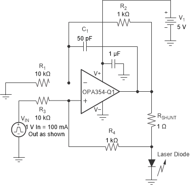
OPA354A-Q1 OPA2354A-Q1 OPA4354-Q1 ai_laser_diode_drvr_bos492.gifFigure 30. Laser Diode Driver

For maximum reliability, TI does not recommend running a continuous DC current greater than ±100 mA; see Figure 20 (Output Voltage Swing vs Output Current). Operate the OPAx354-Q1 family of devices in parallel to supply continuous output currents greater than ±100 mA, as shown in Figure 31.
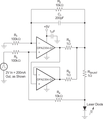
OPA354A-Q1 OPA2354A-Q1 OPA4354-Q1 ai_parallel_operat_bos492.gifFigure 31. Parallel Operation

The OPAx354-Q1 family of devices provides peak currents up to 200 mA, which correspond to the typical short-circuit current. Therefore, an on-chip thermal shutdown circuit protects the OPAx354-Q1 family of devices from dangerously high junction temperatures. At 160°C, the protection circuit shuts down the amplifier. Normal operation resumes when the junction temperature cools below 140°C.