JAJSL77A February 2021 – April 2021 OPA2607-Q1 , OPA607-Q1
PRODUCTION DATA
- 1 特長
- 2 アプリケーション
- 3 概要
- 4 Revision History
- 5 Device Comparison
- 6 Pin Configuration and Functions
- 7 Specifications
- 8 Detailed Description
- 9 Application and Implementation
- 10Power Supply Recommendations
- 11Layout
- 12Device and Documentation Support
- 13Mechanical, Packaging, and Orderable Information
8.3.4 Decompensated Architecture with Wide Gain-Bandwidth Product
Amplifiers such as the OPAx607-Q1 devices are not unity-gain stable are referred to as decompensated amplifiers. The decompensated architecture typically allows for higher GBW, higher slew rate, and lower noise compared to a unity-gain stable amplifier with similar quiescent currents. The increased available bandwidth reduces the rise time and the settling time of the op amp, allowing for sampling at faster rates in an ADC-based signal chain.
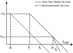
As shown in Figure 8-5, the dominant pole fd is moved to the frequency f1 in the case of a decompensated op amp. The solid AOL plot is the open-loop gain plot of a traditional unity-gain stable op amp. The change in internal compensation in a decompensated amp such as the OPAx607-Q1, increase the bandwidth for the same amount of power. That is, the decompensated op amp has an increased bandwidth to power ratio when compared to a unity-gain stable op amp of equivalent architecture. Besides the advantages in the above mentioned parameters, an increased slew rate and a better distortion (HD2 and HD3) value is achieved because of the higher available loop-gain, compared to its unity-gain counterpart. The most important factor to consider is ensuring that the op amp is in a noise gain (NG) greater than Gmin. A value of NG lower than Gmin results in instability, as shown in Figure 8-5, because the 1/ß curve intersects the AOL curve at 40 dB/decade. This method of analyzing stability is called the rate of closure method. See the precision lab training videos from TI for a better understanding on device stability and for different techniques of ensuring stability.
 Figure 8-5 Gain vs Frequency Characteristics for a Unity-Gain Stable Op Amp and a Decompensated Op Amp
The OPAx607-Q1 devices are stable in a noise gain of 6 V/V (15.56 dB) or higher in conventional gain circuits; see Figure 8-6. The device has 9 MHz of small-signal bandwidth (SSBW) in this gain configuration with approximately 65° of phase margin. The high GBW and low voltage noise of the OPAx607-Q1 devices make them suitable for general-purpose, high-gain applications.