JAJSL77A February 2021 – April 2021 OPA2607-Q1 , OPA607-Q1
PRODUCTION DATA
- 1 特長
- 2 アプリケーション
- 3 概要
- 4 Revision History
- 5 Device Comparison
- 6 Pin Configuration and Functions
- 7 Specifications
- 8 Detailed Description
- 9 Application and Implementation
- 10Power Supply Recommendations
- 11Layout
- 12Device and Documentation Support
- 13Mechanical, Packaging, and Orderable Information
9.2.1.2 Detailed Design Procedure
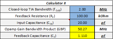
Designs that require high bandwidth from a large area detector with relatively high transimpedance-gain benefit from the low input voltage noise of the OPAx607-Q1 devices. Use the Excel™ calculator available at What You Need To Know About Transimpedance Amplifiers – Part 1 to help with the component selection based on total input capacitance and CTOT. CTOT is referred as CIN in the calculator. CTOT is the sum of CD, CDIFF, and CCM which is 20 pF. Using this value of CTOT, and the targeted closed-loop bandwidth (f–3dB) of 2 MHz and transimpedance gain of 100 kΩ results in amplifier GBW of approximately 50 MHz and a feedback capacitance (CF) of 1.1 pF as shown in Figure 9-2. These results are for a Butterworth response with a Q = 0.707 and a phase margin of approximately 65° which corresponds to 4.3% overshoot.
 Figure 9-2 Results of Inputting Design Parameters in the TIA Calculator
The OPA607-Q1's 50 MHz GBW, is suitable for the above design requirements. If the required feedback capacitance CF comes out to be a very low value capacitor to be practically achievable, a T-Network capacitor circuit as shown below can be used. A very low capacitor value (CEQ) can be achieved between Port1 and Port2 using standard value capacitors in a T-Network circuit as shown in Figure 9-3.
Equation 1.  |
 Figure 9-3 T-Network