JAJSCA3A July   2016  – December 2019 OPA2626

PRODUCTION DATA.  

  1. 特長
  2. アプリケーション
  3. 概要
    1.     Device Images
      1.      SAR ADCドライバ
      2.      高忠実度のトポロジによる動的性能の改善(fIN = 10kHz、1MSPS FFT)
  4. 改訂履歴
  5. Pin Configuration and Functions
    1.     Pin Functions: OPA2626
  6. Specifications
    1. 6.1 Absolute Maximum Ratings
    2. 6.2 ESD Ratings
    3. 6.3 Recommended Operating Conditions
    4. 6.4 Thermal Information
    5. 6.5 Electrical Characteristics: High-Supply
    6. 6.6 Electrical Characteristics: Low-Supply
    7. 6.7 Typical Characteristics
  7. Parameter Measurement Information
    1. 7.1 DC Parameter Measurements
    2. 7.2 Transient Parameter Measurements
    3. 7.3 AC Parameter Measurements
    4. 7.4 Noise Parameter Measurements
  8. Detailed Description
    1. 8.1 Overview
    2. 8.2 Functional Block Diagram
    3. 8.3 Feature Description
      1. 8.3.1 SAR ADC Driver
      2. 8.3.2 Electrical Overstress
    4. 8.4 Device Functional Modes
      1. 8.4.1 High-Drive Mode
  9. Application and Implementation
    1. 9.1 Application Information
    2. 9.2 Typical Applications
      1. 9.2.1 Single-Supply, 16-Bit, 1-MSPS SAR ADC Driver
        1. 9.2.1.1 Design Requirements
        2. 9.2.1.2 Detailed Design Procedure
        3. 9.2.1.3 Application Curve
      2. 9.2.2 Single-Supply, 16-Bit, 1-MSPS, Multiplexed, SAR ADC Driver
        1. 9.2.2.1 Design Requirements
        2. 9.2.2.2 Detailed Design Procedure
        3. 9.2.2.3 Application Curves
  10. 10Power Supply Recommendations
  11. 11Layout
    1. 11.1 Layout Guidelines
    2. 11.2 Layout Example
  12. 12デバイスおよびドキュメントのサポート
    1. 12.1 デバイス・サポート
      1. 12.1.1 開発サポート
        1. 12.1.1.1 TINA-TI(無料のダウンロード・ソフトウェア)
        2. 12.1.1.2 TI Precision Designs
    2. 12.2 ドキュメントのサポート
      1. 12.2.1 関連資料
    3. 12.3 ドキュメントの更新通知を受け取る方法
    4. 12.4 コミュニティ・リソース
    5. 12.5 商標
    6. 12.6 静電気放電に関する注意事項
    7. 12.7 Glossary
  13. 13メカニカル、パッケージ、および注文情報

パッケージ・オプション

メカニカル・データ(パッケージ|ピン)
サーマルパッド・メカニカル・データ
発注情報

AC Parameter Measurements

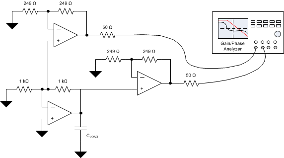
The circuit shown in Figure 56 measures the ac parameters of the OPA2626. Configure V+, V–, and CLOAD as desired. The THS4271 family is used to buffer the input and output of the OPA2626 to prevent loading by the gain phase analyzer. Monitor the input and output voltages on a gain phase analyzer. Use this circuit to measure the gain bandwidth product, and open-loop gain versus frequency versus capacitive load.
OPA2626 AC_Param_Tst_Ckt_sbos690.gifFigure 56. AC-Parameters Measurement Circuit