JAJSFO4B August   2017  – December 2018 OPA2810

PRODUCTION DATA.  

  1. 特長
  2. アプリケーション
    1.     マルチチャネル・センサ・インターフェイス
  3. 概要
    1.     高調波歪みと周波数との関係
  4. 改訂履歴
  5. Pin Configuration and Functions
    1.     Pin Functions
  6. Specifications
    1. 6.1  Absolute Maximum Ratings
    2. 6.2  ESD Ratings
    3. 6.3  Recommended Operating Conditions
    4. 6.4  Thermal Information
    5. 6.5  Electrical Characteristics: 10 V
    6. 6.6  Electrical Characteristics: 24 V
    7. 6.7  Electrical Characteristics: 5 V
    8. 6.8  Typical Characteristics: VS = 10 V
    9. 6.9  Typical Characteristics: VS = 24 V
    10. 6.10 Typical Characteristics: VS = 5 V
    11. 6.11 Typical Characteristics: ±2.375 V to ±12 V Split Supply
  7. Detailed Description
    1. 7.1 Overview
    2. 7.2 Functional Block Diagram
      1. 7.2.1 ESD Protection
    3. 7.3 Feature Description
      1. 7.3.1 OPA2810 Comparison
    4. 7.4 Device Functional Modes
      1. 7.4.1 Split-Supply Operation (±2.375 V to ±13.5 V)
      2. 7.4.2 Single-Supply Operation (4.75 V to 27 V)
  8. Application and Implementation
    1. 8.1 Application Information
      1. 8.1.1 Selection of Feedback Resistors
      2. 8.1.2 Noise Analysis and the Effect of Resistor Elements on Total Noise
    2. 8.2 Typical Applications
      1. 8.2.1 Transimpedance Amplifier
        1. 8.2.1.1 Design Requirements
        2. 8.2.1.2 Detailed Design Procedure
      2. 8.2.2 Multichannel Sensor Interface
  9. Power Supply Recommendations
  10. 10Layout
    1. 10.1 Layout Guidelines
      1. 10.1.1 Thermal Considerations
    2. 10.2 Layout Example
  11. 11デバイスおよびドキュメントのサポート
    1. 11.1 ドキュメントのサポート
      1. 11.1.1 関連資料
    2. 11.2 ドキュメントの更新通知を受け取る方法
    3. 11.3 コミュニティ・リソース
    4. 11.4 商標
    5. 11.5 静電気放電に関する注意事項
    6. 11.6 Glossary
  12. 12メカニカル、パッケージ、および注文情報

パッケージ・オプション

メカニカル・データ(パッケージ|ピン)
サーマルパッド・メカニカル・データ
発注情報

Typical Characteristics: VS = 24 V

at VS+ = 12 V, VS– = –12 V, RL = 1 kΩ, input and output are biased to midsupply, and TA ≈ 25°C. For AC specifications, VO = 2 VPP, G = 2 V/V, RF = 1 kΩ, and CL = 4.7 pF (unless otherwise noted)
OPA2810 D071_SBOS789_SSBW_Vs_Gain_24V.gif
See Figure 65 and Figure 66, VO = 20 mVPP
Figure 19. Noninverting Small-Signal Frequency Response vs Gain
OPA2810 D073_SBOS789_SSBW_Vs_OutputCM_Gain1_47pF_24V.gif
See Figure 65, VO = 20 mVPP, Gain = 1 V/V, CL = 47 pF, RF = 0 Ω
Figure 21. Small-Signal Frequency Response vs Output Common-Mode Voltage
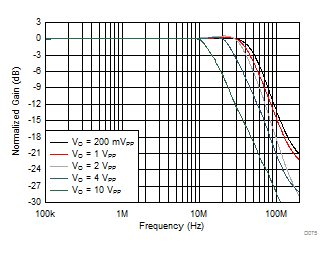
OPA2810 D075_SBOS789_LSBW_Vs_Vout_gain2_24V.gif
See Figure 65, Gain = 2 V/V
Figure 23. Large-Signal Frequency Response vs Vo
OPA2810 D077_SBOS789_HD_Vs_Freq_Vout_G-1_24V.gif
See Figure 66, Gain = –1 V/V
Figure 25. Harmonic Distortion vs Frequency vs Vo
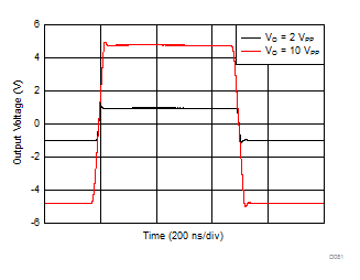
OPA2810 D079_SBOS789_Large_Signal_Transient_Gain1_24V.gif
See Figure 65, Gain = 1 V/V, RF = 0 Ω
Figure 27. Large-Signal Transient Response
OPA2810 D081_SBOS789_Large_Signal_Transient_Gain-1_24V.gif
See Figure 66, Gain = –1 V/V
Figure 29. Large-Signal Transient Response
OPA2810 D083_SBOS789_Input_Overdrive_24V.gif
See Figure 65, Gain = 1 V/V, RF = 0 Ω
Figure 31. Input Overdrive Recovery
OPA2810 D085_SBOS789_Claw_24V.gif
Figure 33. Output Voltage Range vs Load Current
OPA2810 D087_SBOS789_Vos_vs_Vcm.gif
Measured for 34 units
Figure 35. Input Offset Voltage vs Input Common-Mode Voltage
OPA2810 D072_SBOS789_SSBW_Vs_OutputCM_Gain1_33pF_24V.gif
See Figure 65, VO = 20 mVPP, Gain = 1 V/V, CL = 33 pF, RF = 0 Ω
Figure 20. Small-Signal Frequency Response vs Output Common-Mode Voltage
OPA2810 D074_SBOS789_LSBW_Vs_Vout_gain1_24V.gif
See Figure 65, Gain = 1 V/V, RF = 0 Ω
Figure 22. Large-Signal Frequency Response vs Output Voltage
OPA2810 D076_SBOS789_HD_Vs_Freq_Vout_24V.gif
See Figure 65, Gain = 2 V/V
Figure 24. Harmonic Distortion vs Frequency vs Vo
OPA2810 D078_SBOS789_Small_Signal_Transient_200mVpp_24V.gif
See Figure 65, Gain = 1 V/V, RF = 0 Ω
Figure 26. Small-Signal Transient Response
OPA2810 D080_SBOS789_Large_Signal_Transient_Gain2_24V.gif
See Figure 65, Gain = 2 V/V
Figure 28. Large-Signal Transient Response
OPA2810 D082_SBOS789_OvershootUndershoot_Vs_Cout_24V.gif
See Figure 65, Gain = 1 V/V, RF = 0 Ω
Figure 30. Overshoot and Undershoot vs CL
OPA2810 D084_SBOS789_Output_Overdrive_24V.gif
See Figure 66, Gain = –1 V/V
Figure 32. Output Overdrive Recovery
OPA2810 D086_SBOS789_SCCurrent_vs_temp_24V.gif
Output saturated and then short-circuited, Io measured after
TDelay = 5 msec
Figure 34. Output Short-Circuit Current vs Ambient Temperature