SBOS309E August 2004 – December 2024 OPA2830
PRODUCTION DATA
- 1
- 1 Features
- 2 Applications
- 3 Description
- 4 Device Comparison Table
- 5 Pin Configurations and Functions
-
6 Specifications
- 6.1 Absolute Maximum Ratings
- 6.2 ESD Ratings
- 6.3 Recommended Operating Conditions
- 6.4 Thermal Information
- 6.5 Electrical Characteristics VS = ±5V
- 6.6 Electrical Characteristics VS = 5V
- 6.7 Electrical Characteristics VS = 3V
- 6.8 Typical Characteristics: VS = ±5V
- 6.9 Typical Characteristics: VS = ±5V, Differential Configuration
- 6.10 Typical Characteristics: VS = 5V
- 6.11 Typical Characteristics: VS = 5V, Differential Configuration
- 6.12 Typical Characteristics: VS = 3V
- 6.13 Typical Characteristics: VS = 3V, Differential Configuration
- 7 Parameter Measurement Information
-
8 Application and Implementation
- 8.1
Application Information
- 8.1.1 Wideband Voltage-Feedback Operation
- 8.1.2 Single-Supply ADC Interface
- 8.1.3 DC Level-Shifting
- 8.1.4 AC-Coupled Output Video Line Driver
- 8.1.5 Noninverting Amplifier With Reduced Peaking
- 8.1.6 Single-Supply Active Filter
- 8.1.7 Differential Low-Pass Active Filters
- 8.1.8 High-Pass Filters
- 8.1.9 High-Performance DAC Transimpedance Amplifier
- 8.1.10 Operating Suggestions Optimizing Resistor Values
- 8.1.11 Bandwidth vs Gain: Noninverting Operation
- 8.1.12 Inverting Amplifier Operation
- 8.1.13 Output Current and Voltages
- 8.1.14 Driving Capacitive Loads
- 8.1.15 Distortion Performance
- 8.1.16 Noise Performance
- 8.1.17 DC Accuracy and Offset Control
- 8.2 Power Supply Recommendations
- 8.3 Layout
- 8.1
Application Information
- 9 Device and Documentation Support
- 10Revision History
- 11Mechanical, Packaging, and Orderable Information
パッケージ・オプション
デバイスごとのパッケージ図は、PDF版データシートをご参照ください。
メカニカル・データ(パッケージ|ピン)
- D|8
- DGK|8
サーマルパッド・メカニカル・データ
発注情報
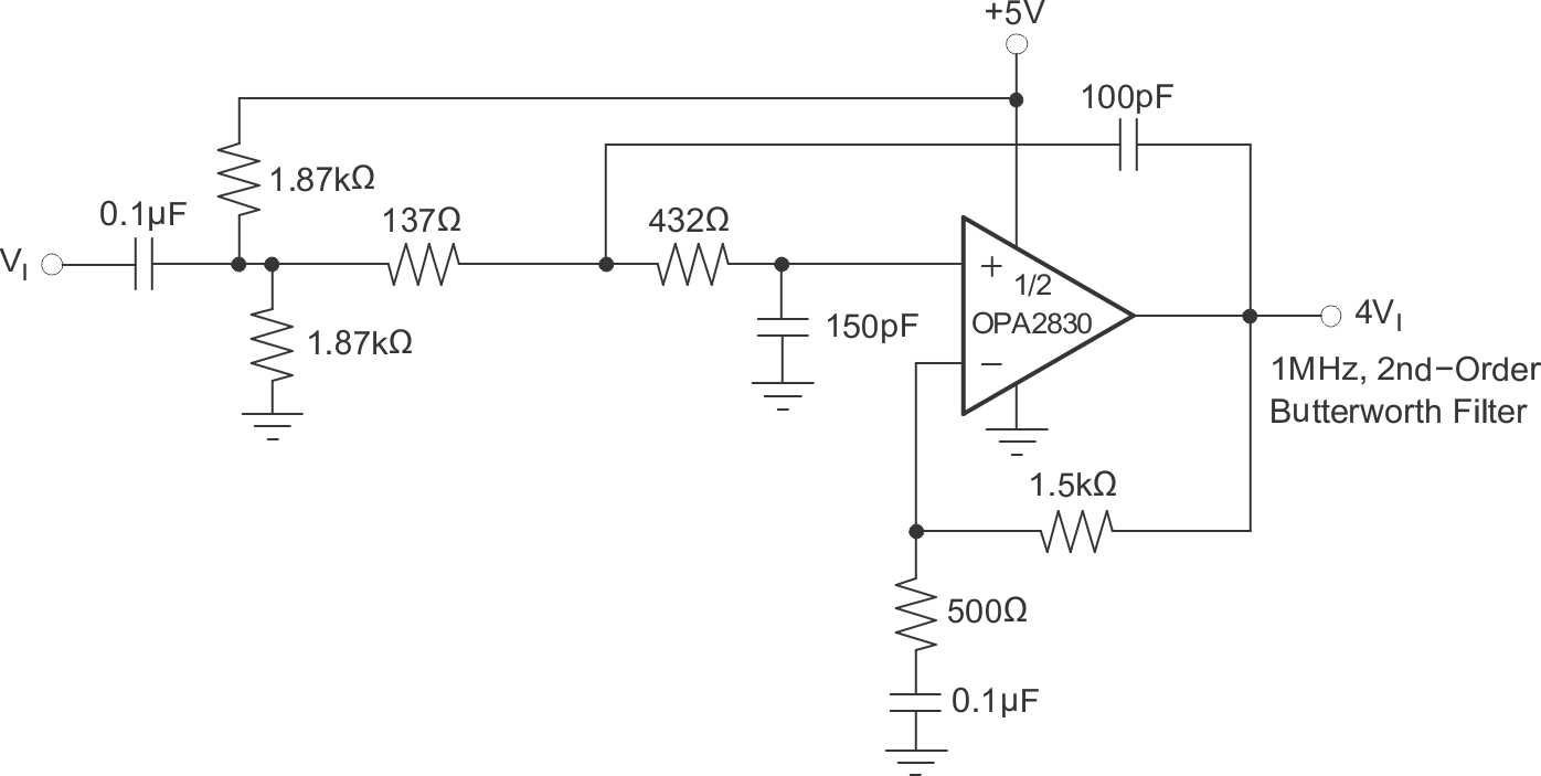
8.1.6 Single-Supply Active Filter
The OPA2830 operating on a single 3V or 5V supply lends well to high-frequency active filter designs. The key additional requirement is to establish the dc operating point of the signal near the supply midpoint for highest dynamic range. Figure 8-9 shows an example design of a 1MHz low-pass Butterworth filter using the Sallen-Key topology.
Both the input signal and the gain setting resistor are ac-coupled using 0.1μF blocking capacitors (actually giving band-pass response with the low-frequency pole set to 32kHz for the component values shown). This configuration allows the midpoint bias formed by the two 1.87kΩ resistors to appear at both the input and output pins. The midband signal gain is set to +4 (12dB) in this case. The capacitor to ground on the noninverting input is intentionally designed at a greater value to dominate input parasitic terms. At a gain of +4, the OPA2830 on a single supply shows 30MHz of small- and large-signal bandwidth. The filter resistor values are slightly adjusted to account for this limited bandwidth in the amplifier stage. Tests of this circuit show a precise 1MHz, –3dB point with a maximally flat pass band (above the 32kHz ac-coupling corner), and a maximum stop-band attenuation of 36dB at the amplifier –3dB bandwidth of 30MHz.
 Figure 8-9 Single-Supply, High-Frequency Active
Filter