JAJSVM5E August 2004 – December 2024 OPA2830
PRODUCTION DATA
- 1
- 1 特長
- 2 アプリケーション
- 3 概要
- 4 Device Comparison Table
- 5 Pin Configurations and Functions
-
6 Specifications
- 6.1 Absolute Maximum Ratings
- 6.2 ESD Ratings
- 6.3 Recommended Operating Conditions
- 6.4 Thermal Information
- 6.5 Electrical Characteristics VS = ±5V
- 6.6 Electrical Characteristics VS = 5V
- 6.7 Electrical Characteristics VS = 3V
- 6.8 Typical Characteristics: VS = ±5V
- 6.9 Typical Characteristics: VS = ±5V, Differential Configuration
- 6.10 Typical Characteristics: VS = 5V
- 6.11 Typical Characteristics: VS = 5V, Differential Configuration
- 6.12 Typical Characteristics: VS = 3V
- 6.13 Typical Characteristics: VS = 3V, Differential Configuration
- 7 Parameter Measurement Information
-
8 Application and Implementation
- 8.1
Application Information
- 8.1.1 Wideband Voltage-Feedback Operation
- 8.1.2 Single-Supply ADC Interface
- 8.1.3 DC Level-Shifting
- 8.1.4 AC-Coupled Output Video Line Driver
- 8.1.5 Noninverting Amplifier With Reduced Peaking
- 8.1.6 Single-Supply Active Filter
- 8.1.7 Differential Low-Pass Active Filters
- 8.1.8 High-Pass Filters
- 8.1.9 High-Performance DAC Transimpedance Amplifier
- 8.1.10 Operating Suggestions Optimizing Resistor Values
- 8.1.11 Bandwidth vs Gain: Noninverting Operation
- 8.1.12 Inverting Amplifier Operation
- 8.1.13 Output Current and Voltages
- 8.1.14 Driving Capacitive Loads
- 8.1.15 Distortion Performance
- 8.1.16 Noise Performance
- 8.1.17 DC Accuracy and Offset Control
- 8.2 Power Supply Recommendations
- 8.3 Layout
- 8.1
Application Information
- 9 Device and Documentation Support
- 10Revision History
- 11Mechanical, Packaging, and Orderable Information
パッケージ・オプション
デバイスごとのパッケージ図は、PDF版データシートをご参照ください。
メカニカル・データ(パッケージ|ピン)
- D|8
- DGK|8
サーマルパッド・メカニカル・データ
発注情報
8.1.7 Differential Low-Pass Active Filters
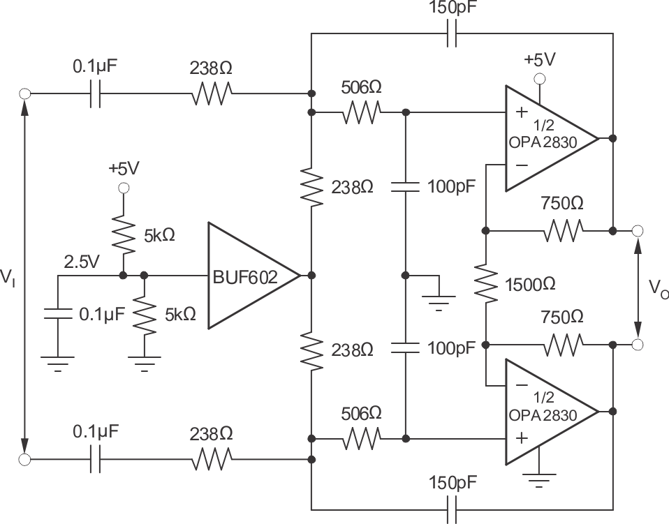
The dual OPA2830 offers an easy way to implement low-power differential active filters. On a single supply, Figure 8-10 shows one way to implement a 2nd-order, low-pass filter. This circuit provides a net differential gain of 1 with a precise 5MHz Butterworth response. The signal is ac-coupled (giving a high-pass pole at low frequencies) with the dc operating point for the circuit set by the unity-gain buffer—the BUF602. This buffer gives a very low output impedance to high frequencies to maintain accurate filter characteristics. If the source is a dc coupled signal already biased into the operating range of the OPA2830 input CMR, these capacitors and the midpoint bias can be removed. To get the desired 5MHz cutoff, the input resistors to the filter is actually 119Ω. This is implemented in Figure 8-10 as the parallel combination of the two 238Ω resistors on each half of the differential input as part of the dc biasing network. If the BUF602 is removed, these resistors must be collapsed back to a single 119Ω input resistor.
 Figure 8-10 Single-Supply, 2nd-Order, Low-Pass Sallen-Key Filter
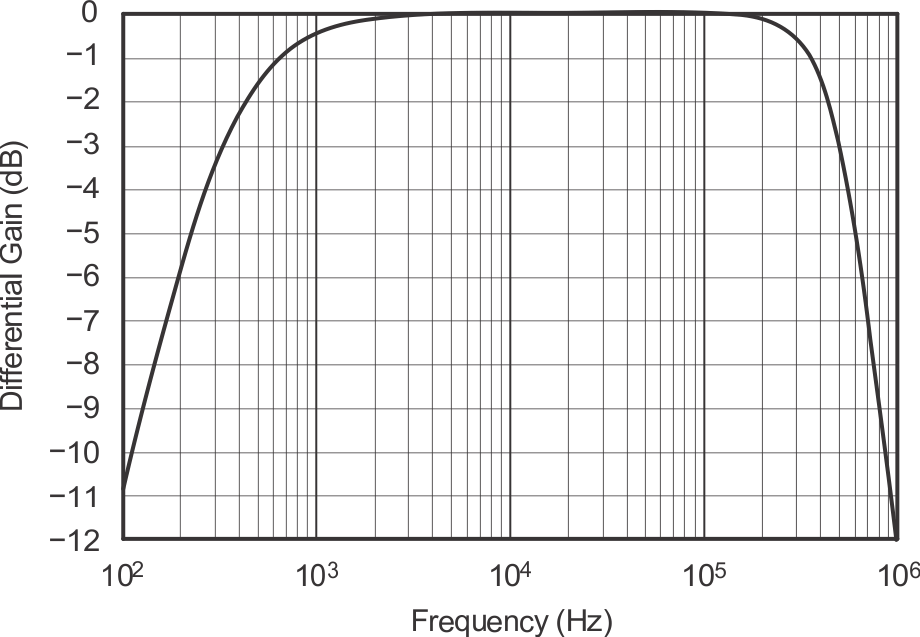
Implementing the dc bias in this way also attenuates the differential signal by half. This attenuation is recovered by setting the amplifier gain at 2V/V to get a net unity-gain filter characteristic from input to output. The filter design shown here has also adjusted the resistor values slightly from an calculated value to account for the 100MHz bandwidth in the amplifier stages. The filter capacitors at the noninverting inputs are shown as two separate capacitors to ground. While that is certainly correct to collapse these two capacitors into a single capacitor across the two inputs (which is 50pF for this circuit) to get the same differential filtering characteristic, tests have shown two separate capacitors to a low impedance point act to attenuate the common-mode feedback present in this circuit giving more stable operation in actual implementation. Figure 8-11 shows the frequency response for the filter of Figure 8-10.
 Figure 8-11 5MHz,
2nd-Order, Butterworth Low-Pass Filter