SBOS309E August 2004 – December 2024 OPA2830
PRODUCTION DATA
- 1
- 1 Features
- 2 Applications
- 3 Description
- 4 Device Comparison Table
- 5 Pin Configurations and Functions
-
6 Specifications
- 6.1 Absolute Maximum Ratings
- 6.2 ESD Ratings
- 6.3 Recommended Operating Conditions
- 6.4 Thermal Information
- 6.5 Electrical Characteristics VS = ±5V
- 6.6 Electrical Characteristics VS = 5V
- 6.7 Electrical Characteristics VS = 3V
- 6.8 Typical Characteristics: VS = ±5V
- 6.9 Typical Characteristics: VS = ±5V, Differential Configuration
- 6.10 Typical Characteristics: VS = 5V
- 6.11 Typical Characteristics: VS = 5V, Differential Configuration
- 6.12 Typical Characteristics: VS = 3V
- 6.13 Typical Characteristics: VS = 3V, Differential Configuration
- 7 Parameter Measurement Information
-
8 Application and Implementation
- 8.1
Application Information
- 8.1.1 Wideband Voltage-Feedback Operation
- 8.1.2 Single-Supply ADC Interface
- 8.1.3 DC Level-Shifting
- 8.1.4 AC-Coupled Output Video Line Driver
- 8.1.5 Noninverting Amplifier With Reduced Peaking
- 8.1.6 Single-Supply Active Filter
- 8.1.7 Differential Low-Pass Active Filters
- 8.1.8 High-Pass Filters
- 8.1.9 High-Performance DAC Transimpedance Amplifier
- 8.1.10 Operating Suggestions Optimizing Resistor Values
- 8.1.11 Bandwidth vs Gain: Noninverting Operation
- 8.1.12 Inverting Amplifier Operation
- 8.1.13 Output Current and Voltages
- 8.1.14 Driving Capacitive Loads
- 8.1.15 Distortion Performance
- 8.1.16 Noise Performance
- 8.1.17 DC Accuracy and Offset Control
- 8.2 Power Supply Recommendations
- 8.3 Layout
- 8.1
Application Information
- 9 Device and Documentation Support
- 10Revision History
- 11Mechanical, Packaging, and Orderable Information
パッケージ・オプション
デバイスごとのパッケージ図は、PDF版データシートをご参照ください。
メカニカル・データ(パッケージ|ピン)
- D|8
- DGK|8
サーマルパッド・メカニカル・データ
発注情報
8.1.16 Noise Performance
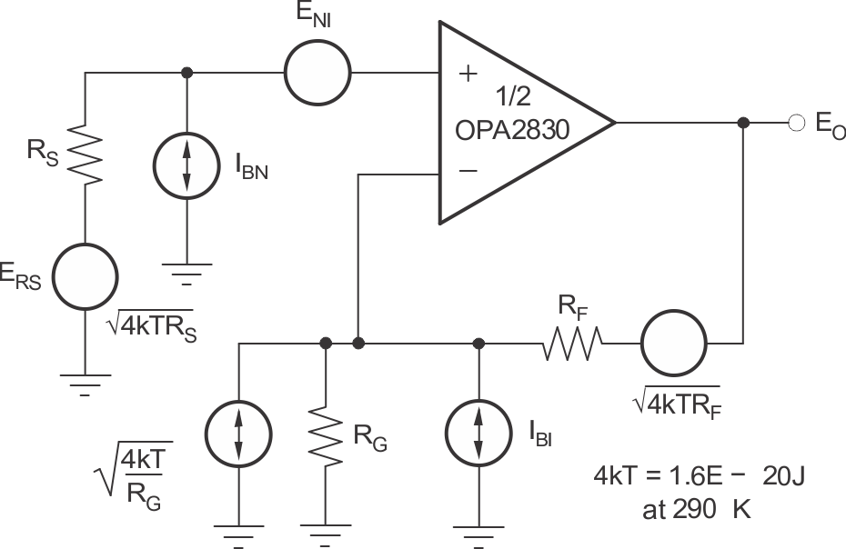
High slew rate, unity-gain stable, voltage-feedback op amps usually achieve a high slew rate at the expense of a higher input noise voltage. However, the 9.2nV/√Hz input voltage noise for the OPA2830 is much less than comparable amplifiers. The input-referred voltage noise and the two input-referred current noise terms (2.8pA/√Hz) combine to give low output noise under a wide variety of operating conditions. Figure 8-16 shows the op-amp noise-analysis model with all the noise terms included. In this model, all noise terms are taken to be noise-voltage or current-density terms in either nV/√Hz or pA/√Hz.
 Figure 8-16 Noise
Analysis Model
Figure 8-16 Noise
Analysis ModelThe total output spot noise voltage is computed as the square root of the sum of all squared output noise voltage contributors. Equation 6 shows the general form for the output noise voltage using the terms shown in Figure 8-16:

Dividing this expression by the noise
gain
(NG = (1 + RF / RG))
gives the equivalent input-referred spot-noise voltage at the noninverting input
shown in Equation 7:

Evaluating these two equations for the circuit and component values shown in Figure 8-1 gives a total-output spot-noise voltage of 19.3nV/√Hz and a total-equivalent-input spot-noise voltage of 9.65nV/√Hz. This result includes the noise added by the resistors. This total input-referred spot noise voltage is not much greater than the 9.2nV/√Hz specification for the op-amp voltage noise alone.