JAJSVM5E August 2004 – December 2024 OPA2830
PRODUCTION DATA
- 1
- 1 特長
- 2 アプリケーション
- 3 概要
- 4 Device Comparison Table
- 5 Pin Configurations and Functions
-
6 Specifications
- 6.1 Absolute Maximum Ratings
- 6.2 ESD Ratings
- 6.3 Recommended Operating Conditions
- 6.4 Thermal Information
- 6.5 Electrical Characteristics VS = ±5V
- 6.6 Electrical Characteristics VS = 5V
- 6.7 Electrical Characteristics VS = 3V
- 6.8 Typical Characteristics: VS = ±5V
- 6.9 Typical Characteristics: VS = ±5V, Differential Configuration
- 6.10 Typical Characteristics: VS = 5V
- 6.11 Typical Characteristics: VS = 5V, Differential Configuration
- 6.12 Typical Characteristics: VS = 3V
- 6.13 Typical Characteristics: VS = 3V, Differential Configuration
- 7 Parameter Measurement Information
-
8 Application and Implementation
- 8.1
Application Information
- 8.1.1 Wideband Voltage-Feedback Operation
- 8.1.2 Single-Supply ADC Interface
- 8.1.3 DC Level-Shifting
- 8.1.4 AC-Coupled Output Video Line Driver
- 8.1.5 Noninverting Amplifier With Reduced Peaking
- 8.1.6 Single-Supply Active Filter
- 8.1.7 Differential Low-Pass Active Filters
- 8.1.8 High-Pass Filters
- 8.1.9 High-Performance DAC Transimpedance Amplifier
- 8.1.10 Operating Suggestions Optimizing Resistor Values
- 8.1.11 Bandwidth vs Gain: Noninverting Operation
- 8.1.12 Inverting Amplifier Operation
- 8.1.13 Output Current and Voltages
- 8.1.14 Driving Capacitive Loads
- 8.1.15 Distortion Performance
- 8.1.16 Noise Performance
- 8.1.17 DC Accuracy and Offset Control
- 8.2 Power Supply Recommendations
- 8.3 Layout
- 8.1
Application Information
- 9 Device and Documentation Support
- 10Revision History
- 11Mechanical, Packaging, and Orderable Information
パッケージ・オプション
デバイスごとのパッケージ図は、PDF版データシートをご参照ください。
メカニカル・データ(パッケージ|ピン)
- D|8
- DGK|8
サーマルパッド・メカニカル・データ
発注情報
8.1.4 AC-Coupled Output Video Line Driver
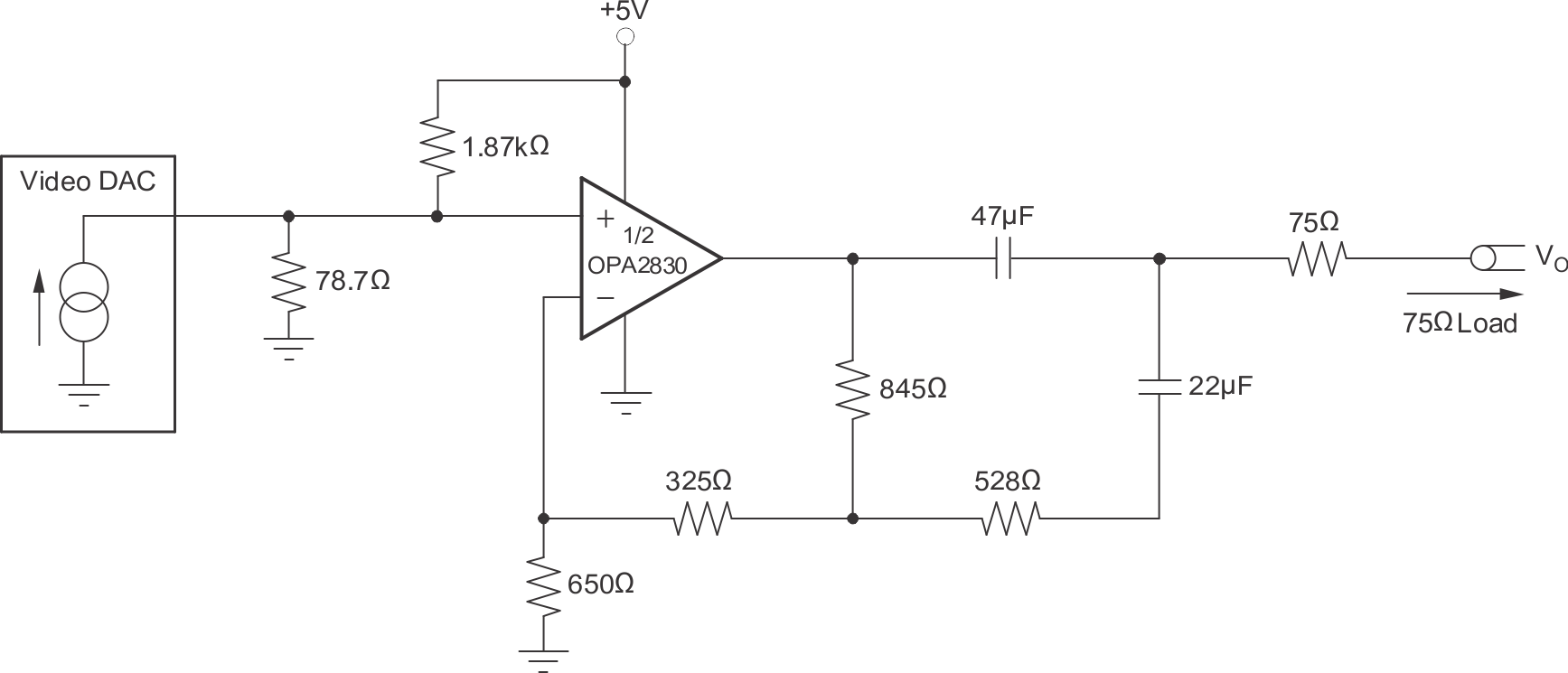
Low-power and low-cost video line drivers often buffer digital-to-analog converter (DAC) outputs with a gain of 2 into a doubly-terminated line. Those interfaces typically require a dc blocking capacitor. For a simple design, that interface often has used a very large value blocking capacitor (220μF) to limit tilt, or SAG, across the frames. Figure 8-7 shows one approach to create a very low high-pass pole location using much lower capacitor values. This circuit gives a voltage gain of 2 at the output pin with a high-pass pole at 8Hz. Given the 150Ω load, a simple blocking capacitor approach requires a 133μF value. The two much-lower-valued capacitors give this same low-pass pole using this simple SAG correction circuit of Figure 8-7.
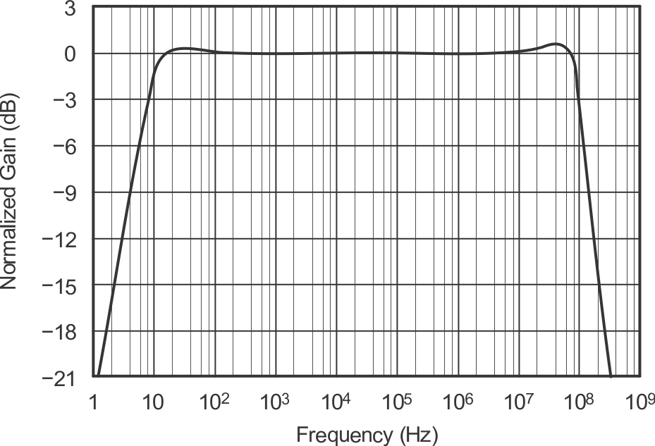
The input is shifted slightly positive in Figure 8-7 using the voltage divider from the positive supply. This shift gives about a 200mV input dc offset that shows up at the output pin as a 400mV dc offset when the DAC output is at zero current during the sync tip portion of the video signal. This offset acts to hold the output in the linear operating region. This configuration passes on any power-supply noise to the output with a gain of approximately –20dB; therefore, good supply decoupling is recommended on the power-supply pin. Figure 8-6 shows the frequency response for the circuit of Figure 8-7. This plot shows the 8Hz low-frequency high-pass pole and a high-end cutoff at approximately 100MHz.
 Figure 8-6 Video-Line-Driver Response to
Matched Load
 Figure 8-7 Video Line Driver With SAG
Correction