JAJSDR3D September 2017 – December 2018 OPA2837 , OPA837
PRODUCTION DATA.
- 1 特長
- 2 アプリケーション
- 3 概要
- 4 改訂履歴
- 5 Pin Configuration and Functions
-
6 Specifications
- 6.1 Absolute Maximum Ratings
- 6.2 ESD Ratings
- 6.3 Recommended Operating Conditions
- 6.4 Thermal Information: OPA837
- 6.5 Thermal Information: OPA2837
- 6.6 Electrical Characteristics: VS = 5 V
- 6.7 Electrical Characteristics: VS = 3 V
- 6.8 Typical Characteristics: VS = 5.0 V
- 6.9 Typical Characteristics: VS = 3.0 V
- 6.10 Typical Characteristics: ±2.5-V to ±1.5-V Split Supply
- 7 Detailed Description
-
8 Application and Implementation
- 8.1
Application Information
- 8.1.1 Noninverting Amplifier
- 8.1.2 Inverting Amplifier
- 8.1.3 Output DC Error Calculations
- 8.1.4 Output Noise Calculations
- 8.1.5 Instrumentation Amplifier
- 8.1.6 Attenuators
- 8.1.7 Differential to Single-Ended Amplifier
- 8.1.8 Differential-to-Differential Amplifier
- 8.1.9 Pulse Application With Single-Supply Circuit
- 8.1.10 ADC Driver Performance
- 8.2 Typical Applications
- 8.1
Application Information
- 9 Power Supply Recommendations
- 10Layout
- 11デバイスおよびドキュメントのサポート
- 12メカニカル、パッケージ、および注文情報
パッケージ・オプション
メカニカル・データ(パッケージ|ピン)
サーマルパッド・メカニカル・データ
- RUN|10
発注情報
8.1.10 ADC Driver Performance
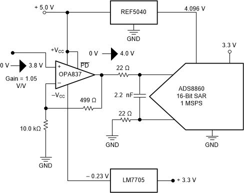
The OPAx837 provides excellent performance when driving high-performance delta-sigma (ΔΣ) or successive-approximation-register (SAR) ADCs in low-power audio and industrial applications.
Figure 82 repeats the front page diagram. Many designs prefer to work with a true 0-V input range to 0-V output at the ADC. The 100-mV output headroom requirement for the OPAx837 then requires a small negative supply to hold the output linearity to ground. This supply is provided in this example using the low-cost LM7705 fixed negative, –0.23-V output regulator. On a 5-V supply, the input headroom requires at least a 1.2-V headroom to that supply. As shown in Figure 82, this requirement limits the maximum input to 3.8 V. The SAR operates with a precision 4.096-V reference provided by the REF5040, where the gain of 1.05 V/V takes the 3.8-V maximum input to a 4.0-V maximum output. The RC values have been set to limit the overshoot at the OPAx837 output pin to reduce clipping on fast (50 ns) transitions.
