SBOS682B May 2013 – June 2016 OPA2317 , OPA317 , OPA4317
PRODUCTION DATA.
- 1 Features
- 2 Applications
- 3 Description
- 4 Revision History
- 5 Pin Configuration and Functions
- 6 Specifications
- 7 Parameter Measurement Information
- 8 Detailed Description
- 9 Application and Implementation
- 10Power Supply Recommendations
- 11Layout
- 12Device and Documentation Support
- 13Mechanical, Packaging, and Orderable Information
パッケージ・オプション
メカニカル・データ(パッケージ|ピン)
サーマルパッド・メカニカル・データ
発注情報
1 Features
- Supply Voltage: 1.8 V to 5.5 V
- microPackages:
- Single: SOT23-5, SC-70, SOIC-8
- Dual: VSSOP-8, SOIC-8
- Quad: SOIC-14, TSSOP-14
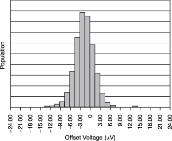
- Low Offset Voltage: 20 μV (Typical)
- CMRR: 108-dB (Typical) PSRR
- Quiescent Current: 35 μA (Maximum)
- Gain Bandwidth: 300 kHz
- Rail-to-Rail Input and Output
- Internal EMI and RFI Filtering
2 Applications
- Battery-Powered Instruments
- Temperature Measurements
- Transducer Applications
- Electronic Scales
- Medical Instrumentation
- Handheld Test Equipment
- Current Sense
3 Description
The OPA317 series of CMOS operational amplifiers offer precision performance at a very competitive price. These devices are members of the Zerø-Drift family of amplifiers that use a proprietary autocalibration technique to simultaneously provide low offset voltage (90 μV maximum) and near-zero drift over time and temperature at only 35 μA (maximum) of quiescent current.
The OPA317 family features rail-to-rail input and output in addition to near flat 1/f noise, making this amplifier ideal for many applications, and much easier to design into a system. These devices are optimized for low-voltage operation as low as 1.8 V (±0.9 V) and up to 5.5 V (±2.75 V).
The OPA317 (single version) is available in the SC70-5, SOT23-5, and SOIC-8 packages. The OPA2317 (dual version) is offered in the VSSOP-8 and SOIC-8 packages. The OPA4317 is offered in the standard SOIC-14 and TSSOP-14 packages. All versions are specified for operation from –40°C to +125°C.
Device Information(1)
| PART NUMBER | PACKAGE | BODY SIZE (NOM) |
|---|---|---|
| OPA317 | SOIC (8) | 3.91 mm × 4.90 mm |
| SOT-23 (5) | 1.60 mm × 2.90 mm | |
| SC70 (5) | 1.25 mm × 2.00 mm | |
| OPA2317 | SOIC (8) | 3.91 mm × 4.90 mm |
| VSSOP (8) | 3.00 mm × 3.00 mm | |
| OPA4317 | SOIC (14) | 3.91 mm × 8.65 mm |
| TSSOP (14) | 4.40 mm × 5.00 mm |
- For all available packages, see the orderable addendum at the end of the data sheet.
Distribution of Offset Voltage
