JAJSGR4B September   2014  – December 2018 OPA2320-Q1 , OPA320-Q1

PRODUCTION DATA.  

  1. 特長
  2. アプリケーション
    1.     ゼロ・クロスオーバー歪み:低オフセット電圧
  3. 概要
  4. 改訂履歴
  5. Pin Configuration and Functions
    1.     Pin Functions
  6. Specifications
    1. 6.1 Absolute Maximum Ratings
    2. 6.2 ESD Ratings
    3. 6.3 Recommended Operating Conditions
    4. 6.4 Thermal Information
    5. 6.5 Electrical Characteristics:
    6. 6.6 Typical Characteristics
  7. Detailed Description
    1. 7.1 Overview
    2. 7.2 Functional Block Diagram
    3. 7.3 Feature Description
      1. 7.3.1 Input and ESD Protection
      2. 7.3.2 Feedback Capacitor Improves Response
      3. 7.3.3 EMI Susceptibility And Input Filtering
      4. 7.3.4 Output Impedance
      5. 7.3.5 Capacitive Load and Stability
      6. 7.3.6 Overload Recovery Time
    4. 7.4 Device Functional Modes
      1. 7.4.1 Rail-to-Rail Input
      2. 7.4.2 Phase Reversal
  8. Application and Implementation
    1. 8.1 Application Information
    2. 8.2 Typical Applications
      1. 8.2.1 Transimpedance Amplifier
        1. 8.2.1.1 Design Requirements
        2. 8.2.1.2 Detailed Design Procedure
          1. 8.2.1.2.1 Optimizing The Transimpedance Circuit
        3. 8.2.1.3 Application Curves
      2. 8.2.2 High-Impedance Sensor Interface
      3. 8.2.3 Driving ADCs
      4. 8.2.4 Active Filter
  9. Power Supply Recommendations
  10. 10Layout
    1. 10.1 Layout Guidelines
    2. 10.2 Layout Example
  11. 11デバイスおよびドキュメントのサポート
    1. 11.1 デバイス・サポート
      1. 11.1.1 開発サポート
    2. 11.2 関連リンク
    3. 11.3 ドキュメントの更新通知を受け取る方法
    4. 11.4 コミュニティ・リソース
    5. 11.5 商標
    6. 11.6 静電気放電に関する注意事項
    7. 11.7 Glossary
  12. 12メカニカル、パッケージ、および注文情報

パッケージ・オプション

メカニカル・データ(パッケージ|ピン)
サーマルパッド・メカニカル・データ
発注情報

Typical Characteristics

at TA = 25°C, V(CM) = VO = mid-supply, and R(L) = 10 kΩ (unless otherwise noted)
OPA320-Q1 OPA2320-Q1 tc_histo_voff_slos884.gif
Figure 1. Offset Voltage Production Distribution
OPA320-Q1 OPA2320-Q1 tc_vo-vcm_slos884.gif
Representative units, VS = ±2.75 V
Figure 3. Offset Voltage vs Common-Mode Voltage
OPA320-Q1 OPA2320-Q1 tc_oloop_g-tmp_slos884.gif
Figure 5. Open-Loop Gain vs Temperature
OPA320-Q1 OPA2320-Q1 tc_ibc-vs_slos884.gif
Figure 7. Input Bias Current vs Supply Voltage
OPA320-Q1 OPA2320-Q1 tc_histo_ibias_slos884.gif
Figure 9. Input Bias Current Distribution
OPA320-Q1 OPA2320-Q1 tc_cmrr_psrr-frq_slos884.gif
Figure 11. CMRR and PSRR vs Frequency
OPA320-Q1 OPA2320-Q1 tc_noise_density_slos884.gif
VS = 1.8 to 5.5 V
Figure 13. Input Voltage Noise Spectral Density vs Frequency
OPA320-Q1 OPA2320-Q1 tc_cloop-frq_18v_slos884.gif
VS = 1.8 V, C(L) = 50 pF, R(L) = 10 kΩ
Figure 15. Closed-Loop Gain vs Frequency
OPA320-Q1 OPA2320-Q1 tc_max_vo-frq_slos884.gif
C(L) = 50 pF, R(L) = 10 kΩ
Figure 17. Maximum Output Voltage vs Frequency
OPA320-Q1 OPA2320-Q1 tc_oloop_imp-frq_slos884.gif
VS = ±2.75 V
Figure 19. Open-Loop Output Impedance vs Frequency
OPA320-Q1 OPA2320-Q1 tc_thdn-amp_slos884.gif
VS = ±2.5 V, f = 10 kHz, G = 1 V/V
Figure 21. THD+N vs Amplitude
OPA320-Q1 OPA2320-Q1 tc_thdn-frq_4vin_slos884.gif
VS = ±2.5 V, f = 10 kHz, G = 1 V/V, VI = 4 VPP
Figure 23. THD+N vs Frequency
OPA320-Q1 OPA2320-Q1 tc_sr-vs_slos884.gif
C(L) = 50 pF
Figure 25. Slew Rate vs Supply Voltage
OPA320-Q1 OPA2320-Q1 tc_sm_step_neg_slos884.gif
VS = ±2.75 V, G = –1 V/V, VI = 100 mVPP
Figure 27. Small-Signal Step Response
OPA320-Q1 OPA2320-Q1 tc_histo_voff_drift_slos884.gif
Figure 2. Offset Voltage Drift Distribution
OPA320-Q1 OPA2320-Q1 tc_oloop_g_ph-frq_slos884.gif
VS = ±2.5 V, C(L) = 50 pF
Figure 4. Open-Loop Gain and Phase vs Frequency
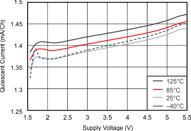
OPA320-Q1 OPA2320-Q1 tc_iq-vs_slos884.gif
Figure 6. Quiescent Current vs Supply Voltage
OPA320-Q1 OPA2320-Q1 tc_ibc-vcm_slos884.gif
Figure 8. Input Bias Current vs Common-Mode Voltage
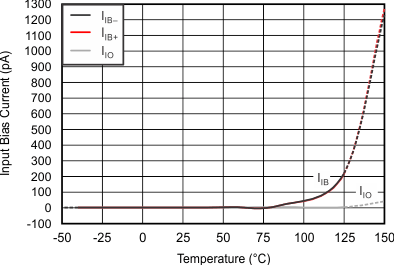
OPA320-Q1 OPA2320-Q1 tc_ibc-tmp_slos884.gif
Figure 10. Input Bias Current vs Temperature
OPA320-Q1 OPA2320-Q1 tc_cmrr_psrr-tmp_slos884.gif
VS = 1.8 to 5.5 V
Figure 12. CMRR and PSRR vs Temperature
OPA320-Q1 OPA2320-Q1 tc_vin_noise_slos884.gif
Figure 14. 0.1-Hz to 10-Hz Input Voltage Noise
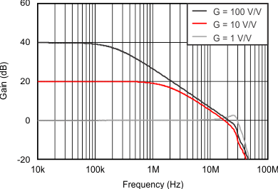
OPA320-Q1 OPA2320-Q1 tc_cloop-frq_55v_slos884.gif
VS = 5.5 V, C(L) = 50 pF, R(L) = 10 kΩ
Figure 16. Closed-Loop Gain vs Frequency
OPA320-Q1 OPA2320-Q1 tc_vo-io_slos884.gif
VS = ±2.75 V
Figure 18. Output Voltage Swing vs Output Current
OPA320-Q1 OPA2320-Q1 tc_oshoot-cl_slos884.gif
Figure 20. Small-Signal Overshoot vs Load Capacitance
OPA320-Q1 OPA2320-Q1 tc_thdn-frq_2vin_slos884.gif
VS = ±2.5 V, f = 10 kHz, G = 1 V/V, VI = 2 VPP
Figure 22. THD+N vs Frequency
OPA320-Q1 OPA2320-Q1 tc_ch_sep-frq_slos884.gif
VS = ±2.75 V
Figure 24. Channel Separation vs Frequency
OPA320-Q1 OPA2320-Q1 tc_sm_step_pos_slos884.gif
VS = ±2.75 V, G = 1 V/V, VI = 100 mVPP
Figure 26. Small-Signal Step Response
OPA320-Q1 OPA2320-Q1 tc_lg_step_resp_slos884.gif
VS = ±2.75 V, G = 1 V/V, VI = 2 VPP
Figure 28. Large-Signal Step Response vs Time