JAJSF99G March   2002  – April 2018 OPA2354 , OPA354 , OPA4354

PRODUCTION DATA.  

  1. 特長
  2. アプリケーション
  3. 概要
    1.     Device Images
      1.      概略回路図
  4. 改訂履歴
  5. Device Comparison Table
  6. Pin Configuration and Functions
    1.     Pin Functions: OPA354
    2.     Pin Functions: OPA2354
    3.     Pin Functions: OPA4354
  7. Specifications
    1. 7.1 Absolute Maximum Ratings
    2. 7.2 ESD Ratings
    3. 7.3 Recommended Operating Conditions
    4. 7.4 Thermal Information: OPA354
    5. 7.5 Thermal Information: OPA2354
    6. 7.6 Thermal Information: OPA4354
    7. 7.7 Electrical Characteristics: VS = 2.7 V to 5.5 V (Single-Supply)
    8. 7.8 Typical Characteristics
  8. Detailed Description
    1. 8.1 Overview
    2. 8.2 Functional Block Diagram
    3. 8.3 Feature Description
      1. 8.3.1 Operating Voltage
      2. 8.3.2 Rail-to-Rail Input
      3. 8.3.3 Rail-to-Rail Output
      4. 8.3.4 Output Drive
      5. 8.3.5 Video
      6. 8.3.6 Driving Analog-to-Digital converters
      7. 8.3.7 Capacitive Load and Stability
      8. 8.3.8 Wideband Transimpedance Amplifier
    4. 8.4 Device Functional Modes
  9. Application and Implementation
    1. 9.1 Application Information
    2. 9.2 Typical Application
      1. 9.2.1 Design Requirements
      2. 9.2.2 Detailed Design Procedure
        1. 9.2.2.1 Optimizing the Transimpedance Circuit
      3. 9.2.3 Application Curve
  10. 10Power Supply Recommendations
  11. 11Layout
    1. 11.1 Layout Guidelines
    2. 11.2 Layout Example
    3. 11.3 Power Dissipation
    4. 11.4 PowerPAD Thermally-Enhanced Package
    5. 11.5 PowerPAD Assembly Process
  12. 12デバイスおよびドキュメントのサポート
    1. 12.1 ドキュメントのサポート
    2. 12.2 関連リンク
    3. 12.3 ドキュメントの更新通知を受け取る方法
    4. 12.4 コミュニティ・リソース
    5. 12.5 商標
    6. 12.6 静電気放電に関する注意事項
    7. 12.7 Glossary
  13. 13メカニカル、パッケージ、および注文情報

パッケージ・オプション

メカニカル・データ(パッケージ|ピン)
サーマルパッド・メカニカル・データ
発注情報

Typical Application

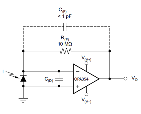
Wide gain bandwidth, low input bias current, low input voltage, and current noise make the OPAx354 family of devices an ideal wideband photodiode transimpedance amplifier. Low-voltage noise is important because photodiode capacitance causes the effective noise gain of the circuit to increase at high frequency. The key elements to a transimpedance design, as shown in Figure 37, are the expected diode capacitance, (which include the parasitic input common-mode and differential-mode input capacitance) the desired transimpedance gain, and the gain-bandwidth (GBW) for the OPAx354 family of devices (20 MHz). With these three variables set, the feedback capacitor value is set to control the frequency response. Feedback capacitance includes the stray capacitance , which is 0.2 pF for a typical surface-mount resistor.
OPA354 OPA2354 OPA4354 Transimp_Amp_bos233.gifFigure 37. Dual-Supply Transimpedance Amplifier