JAJSF79F March   2002  – April 2018 OPA2357 , OPA357

PRODUCTION DATA.  

  1. 特長
  2. アプリケーション
  3. 概要
    1.     Device Images
      1.      概略回路図
  4. 改訂履歴
  5. Pin Configuration and Functions
    1.     Pin Functions
  6. Specifications
    1. 6.1 Absolute Maximum Ratings
    2. 6.2 ESD Ratings
    3. 6.3 Recommended Operating Conditions
    4. 6.4 Thermal Information
    5. 6.5 Electrical Characteristics: VS = +2.7-V to +5.5-V Single-Supply
    6. 6.6 Typical Characteristics
  7. Detailed Description
    1. 7.1 Overview
    2. 7.2 Functional Block Diagram
    3. 7.3 Feature Description
      1. 7.3.1  OPAx357 Comparison
      2. 7.3.2  Operating Voltage
      3. 7.3.3  Enable Function
      4. 7.3.4  Rail-to-Rail Input
      5. 7.3.5  Rail-to-Rail Output
      6. 7.3.6  Output Drive
      7. 7.3.7  Video
      8. 7.3.8  Wideband Video Multiplexing
      9. 7.3.9  Driving Analog-to-Digital Converters
      10. 7.3.10 Capacitive Load and Stability
      11. 7.3.11 Wideband Transimpedance Amplifier
    4. 7.4 Device Functional Modes
  8. Application and Implementation
    1. 8.1 Application Information
    2. 8.2 Typical Applications
      1. 8.2.1 Transimpedance Amplifier
        1. 8.2.1.1 Design Requirements
        2. 8.2.1.2 Detailed Design Procedure
          1. 8.2.1.2.1 Custom Design With WEBENCH® Tools
          2. 8.2.1.2.2 OPAx357 Design Procedure
            1. 8.2.1.2.2.1 Optimizing the Transimpedance Circuit
        3. 8.2.1.3 Application Curve
      2. 8.2.2 High-Impedance Sensor Interface
      3. 8.2.3 Driving ADCs
      4. 8.2.4 Active Filter
  9. Power Supply Recommendations
    1. 9.1 Power Dissipation
  10. 10Layout
    1. 10.1 Layout Guidelines
    2. 10.2 Layout Example
  11. 11デバイスおよびドキュメントのサポート
    1. 11.1 デバイス・サポート
      1. 11.1.1 開発サポート
        1. 11.1.1.1 WEBENCH®ツールによるカスタム設計
    2. 11.2 ドキュメントのサポート
      1. 11.2.1 関連資料
    3. 11.3 関連リンク
    4. 11.4 ドキュメントの更新通知を受け取る方法
    5. 11.5 コミュニティ・リソース
    6. 11.6 商標
    7. 11.7 静電気放電に関する注意事項
    8. 11.8 Glossary
  12. 12メカニカル、パッケージ、および注文情報

パッケージ・オプション

メカニカル・データ(パッケージ|ピン)
サーマルパッド・メカニカル・データ
発注情報

Driving Analog-to-Digital Converters

The OPA357 series op amps offer 60 ns of settling time to 0.01%, making the series a good choice for driving high- and medium-speed sampling A/D converters and reference circuits. The OPA357 series provides an effective means of buffering the A/D converter input capacitance and resulting charge injection while providing signal gain.

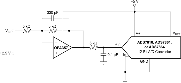
Figure 38 shows the OPA357 driving an A/D converter. With the OPA357 in an inverting configuration, a capacitor across the feedback resistor can be used to filter high-frequency noise in the signal, as shown in Figure 38.
OPA357 OPA2357 OPA357_SBOS235_inverting_configuration_driving_adc.gif

NOTE:

A/D converter input = 0 V to VREF.

NOTE:

VIN = 0 V to –5 V for a 0-V to 5-V output.
Figure 38. The OPA357 in Inverting Configuration Driving an A/D Converter