JAJSF79F March 2002 – April 2018 OPA2357 , OPA357
PRODUCTION DATA.
- 1 特長
- 2 アプリケーション
- 3 概要
- 4 改訂履歴
- 5 Pin Configuration and Functions
- 6 Specifications
-
7 Detailed Description
- 7.1 Overview
- 7.2 Functional Block Diagram
- 7.3
Feature Description
- 7.3.1 OPAx357 Comparison
- 7.3.2 Operating Voltage
- 7.3.3 Enable Function
- 7.3.4 Rail-to-Rail Input
- 7.3.5 Rail-to-Rail Output
- 7.3.6 Output Drive
- 7.3.7 Video
- 7.3.8 Wideband Video Multiplexing
- 7.3.9 Driving Analog-to-Digital Converters
- 7.3.10 Capacitive Load and Stability
- 7.3.11 Wideband Transimpedance Amplifier
- 7.4 Device Functional Modes
- 8 Application and Implementation
- 9 Power Supply Recommendations
- 10Layout
- 11デバイスおよびドキュメントのサポート
- 12メカニカル、パッケージ、および注文情報
8.2.1.2.2 OPAx357 Design Procedure
To achieve a maximally-flat, second-order Butterworth frequency response, set the feedback pole using Equation 3.

Calculate the bandwidth using Equation 4.

For other transimpedance bandwidths, consider the high-speed CMOS OPA380 (90-MHz GBW), OPA354
(100-MHz GBW), OPA300 (180-MHz GBW), OPA355 (200-MHz GBW), or OPA656 and OPA657 (400-MHz GBW).
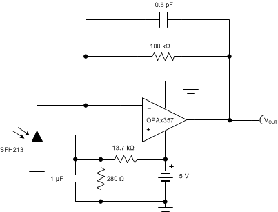
For single-supply applications, the +INx input can be biased with a positive DC voltage to allow the output to reach true zero when the photodiode is not exposed to any light, and respond without the added delay that results from coming out of the negative rail; Figure 42 shows this configuration. This bias voltage appears across the photodiode, providing a reverse bias for faster operation.
 Figure 42. Single-Supply Transimpedance Amplifier
 For additional information, see the Compensate Transimpedance Amplifiers Intuitively application bulletin.