JAJSF79F March 2002 – April 2018 OPA2357 , OPA357
PRODUCTION DATA.
- 1 特長
- 2 アプリケーション
- 3 概要
- 4 改訂履歴
- 5 Pin Configuration and Functions
- 6 Specifications
-
7 Detailed Description
- 7.1 Overview
- 7.2 Functional Block Diagram
- 7.3
Feature Description
- 7.3.1 OPAx357 Comparison
- 7.3.2 Operating Voltage
- 7.3.3 Enable Function
- 7.3.4 Rail-to-Rail Input
- 7.3.5 Rail-to-Rail Output
- 7.3.6 Output Drive
- 7.3.7 Video
- 7.3.8 Wideband Video Multiplexing
- 7.3.9 Driving Analog-to-Digital Converters
- 7.3.10 Capacitive Load and Stability
- 7.3.11 Wideband Transimpedance Amplifier
- 7.4 Device Functional Modes
- 8 Application and Implementation
- 9 Power Supply Recommendations
- 10Layout
- 11デバイスおよびドキュメントのサポート
- 12メカニカル、パッケージ、および注文情報
8.2.3 Driving ADCs
The OPAx357 op amps are designed for driving sampling analog-to-digital (A/D) converters with sampling speeds up to 1 MSPS. The zero-crossover distortion input stage topology allows the OPAx357 family of devices to drive A/D converters without degradation of differential linearity and THD.
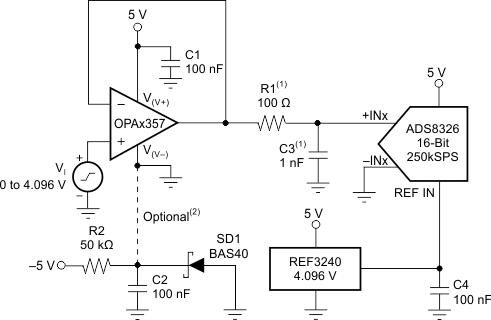
The OPAx357 family of devices can be used to buffer the A/D converter switched input capacitance and resulting charge injection while providing signal gain. Figure 45 shows the OPAx357 family of devices configured to drive the ADS8326.

1.
NOINDENT:
Suggested value; may require adjustment based on specific application.2.
Figure 45. Driving the ADS8326 NOINDENT:
Single-supply applications lose a small number of A/D converter codes near ground as a result of op amp output swing limitation. If a negative power supply is available, this simple circuit creates a –0.3-V supply to allow output swing to true ground potential.