SBOS641D June 2012 – September 2016 OPA4188
PRODUCTION DATA.
- 1 Features
- 2 Applications
- 3 Description
- 4 Revision History
- 5 Zero-Drift Amplifier Portfolio
- 6 Pin Configuration and Functions
-
7 Specifications
- 7.1 Absolute Maximum Ratings
- 7.2 ESD Ratings
- 7.3 Recommended Operating Conditions
- 7.4 Thermal Information
- 7.5 Electrical Characteristics: High-Voltage Operation, VS = ±4 V to ±18 V (VS = 8 V to 36 V)
- 7.6 Electrical Characteristics: Low-Voltage Operation, VS = ±2 V to < ±4 V (VS = +4 V to < +8 V)
- 7.7 Typical Characteristics
- 8 Detailed Description
- 9 Applications and Implementation
- 10Power Supply Recommendations
- 11Layout
- 12Device and Documentation Support
- 13Mechanical, Packaging, and Orderable Information
パッケージ・オプション
メカニカル・データ(パッケージ|ピン)
サーマルパッド・メカニカル・データ
発注情報
VS = ±18 V, VCM = VS / 2, RLOAD = 10 kΩ connected to VS / 2, and CL = 100 pF, unless otherwise noted.
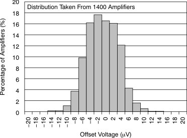 Figure 1. Offset Voltage Production Distribution
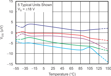 Figure 3. Offset Voltage vs Temperature
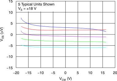 Figure 5. Offset Voltage vs Common-Mode Voltage
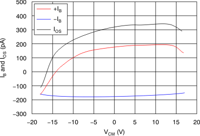 Figure 7. IB and IOS vs Common-Mode Voltage
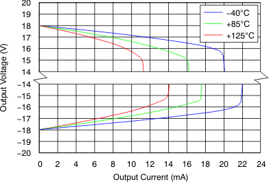 Figure 9. Output Voltage Swing vs Output Current (Maximum Supply)
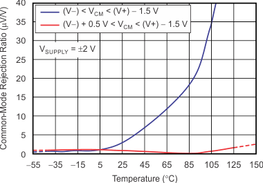 Figure 11. CMRR vs Temperature
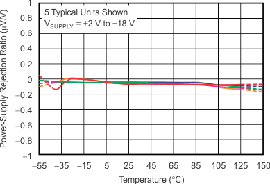 Figure 13. PSRR vs Temperature
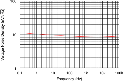 Figure 15. Input Voltage Noise Spectral Density vs Frequency
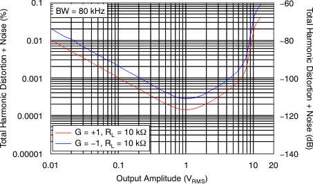 Figure 17. THD+N vs Output Amplitude
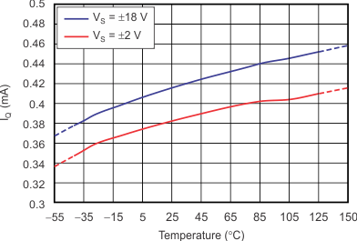 Figure 19. Quiescent Current vs Temperature
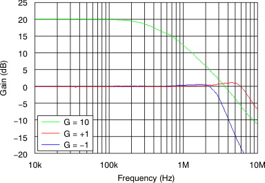 Figure 21. Closed-Loop Gain vs Frequency
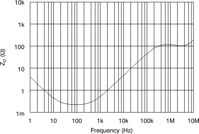 Figure 23. Open-Loop Output Impedance vs Frequency
 Figure 25. Small-Signal Overshoot vs Capacitive Load
(100-mV Output Step)
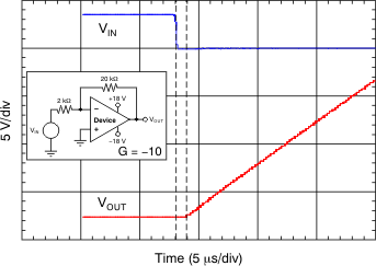
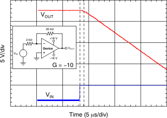 Figure 27. Positive Overload Recovery
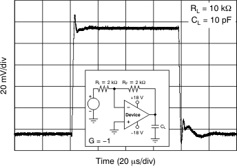
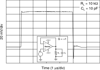 Figure 29. Small-Signal Step Response (100 mV)
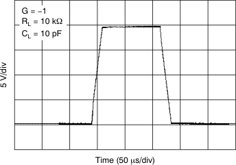
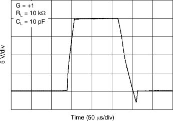 Figure 31. Large-Signal Step Response
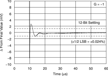
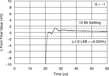 Figure 33. Large-Signal Settling Time (10-V Positive Step)
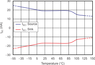 Figure 35. Short Circuit Current vs Temperature
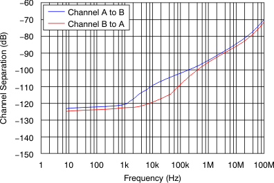 Figure 37. Channel Separation vs Frequency
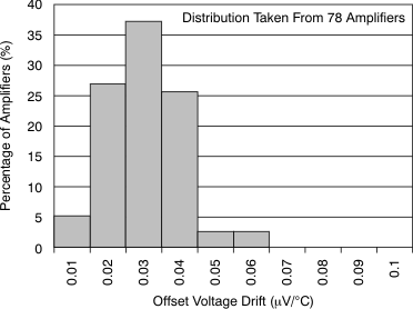 Figure 2. Offset Voltage Drift Distribution
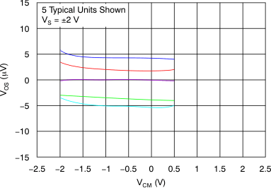 Figure 4. Offset Voltage vs Common-Mode Voltage
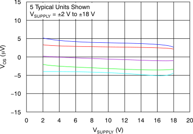 Figure 6. Offset Voltage vs Power Supply
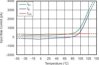 Figure 8. Input Bias Current vs Temperature
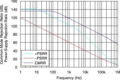 Figure 10. CMRR and PSRR vs Frequency
(Referred-to-Input)
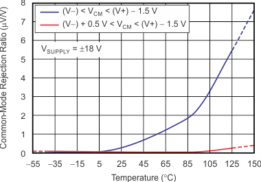 Figure 12. CMRR vs Temperature
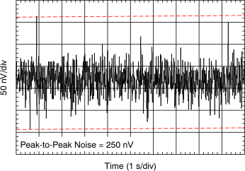 Figure 14. 0.1-Hz to 10-Hz Noise
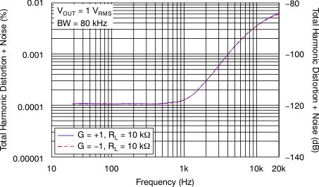 Figure 16. THD+N Ratio vs Frequency
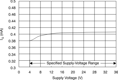 Figure 18. Quiescent Current vs Supply Voltage
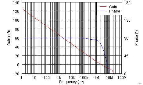 Figure 20. Open-Loop Gain and Phase vs Frequency
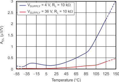 Figure 22. Open-Loop Gain vs Temperature
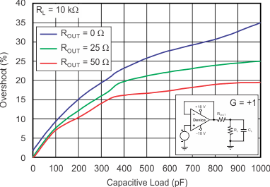 Figure 24. Small-Signal Overshoot vs Capacitive Load
(100-mV Output Step)
 Figure 26. No Phase Reversal
 Figure 28. Negative Overload Recovery
 Figure 30. Small-Signal Step Response (100 mV)
 Figure 32. Large-Signal Step Response
 Figure 34. Large-Signal Settling Time (10-V Negative Step)
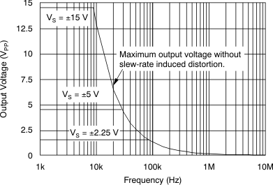
 Figure 36. Maximum Output Voltage vs Frequency
 Figure 38. EMIRR IN+ vs Frequency


(100-mV Output Step)


(Referred-to-Input)


(100-mV Output Step)

