JAJSEY8A
March 2018 – January 2021
OPA197-Q1
,
OPA2197-Q1
,
OPA4197-Q1
PRODUCTION DATA
1
特長
2
アプリケーション
3
概要
4
Revision History
5
Pin Configuration and Functions
6
Specifications
6.1
Absolute Maximum Ratings
6.2
ESD Ratings
6.3
Recommended Operating Conditions
6.4
Thermal Information: OPA197-Q1
6.5
Thermal Information: OPA2197-Q1
6.6
Thermal Information: OPA4197-Q1
6.7
Electrical Characteristics: VS = ±4 V to ±18 V (VS = 8 V to 36 V)
6.8
Electrical Characteristics: VS = ±2.25 V to ±4 V (VS = 4.5 V to 8 V)
6.9
Typical Characteristics
7
Detailed Description
7.1
Overview
7.2
Functional Block Diagram
7.3
Feature Description
7.3.1
Input Protection Circuitry
7.3.2
EMI Rejection
7.3.3
Phase Reversal Protection
7.3.4
Thermal Protection
7.3.5
Capacitive Load and Stability
7.3.6
Common-Mode Voltage Range
7.3.7
Electrical Overstress
7.3.8
Overload Recovery
7.4
Device Functional Modes
8
Application and Implementation
8.1
Application Information
8.2
Typical Applications
8.2.1
16-Bit Precision Multiplexed Data-Acquisition System
8.2.1.1
Design Requirements
8.2.1.2
Detailed Design Procedure
8.2.1.3
Application Curve
8.2.2
Slew-Rate Limit for Input Protection
8.2.3
Precision Reference Buffer
9
Power Supply Recommendations
10
Layout
10.1
Layout Guidelines
10.2
Layout Examples
11
Device and Documentation Support
11.1
Device Support
11.1.1
Development Support
11.1.1.1
TINA-TI™ Simulation Software (Free Download)
11.1.1.2
TI Precision Designs
11.2
Documentation Support
11.2.1
Related Documentation
11.3
ドキュメントの更新通知を受け取る方法
11.4
サポート・リソース
11.5
Trademarks
11.6
静電気放電に関する注意事項
11.7
用語集
12
Mechanical, Packaging, and Orderable Information
パッケージ・オプション
メカニカル・データ(パッケージ|ピン)
PW|14
MPDS360A
サーマルパッド・メカニカル・データ
発注情報
jajsey8a_oa
jajsey8a_pm
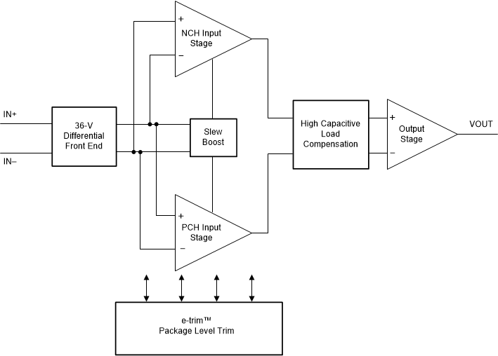
7.2
Functional Block Diagram