JAJSEY7C January 2016 – March 2018 OPA197 , OPA2197 , OPA4197
PRODUCTION DATA.
- 1 特長
- 2 アプリケーション
- 3 概要
- 4 改訂履歴
- 5 Pin Configuration and Functions
-
6 Specifications
- 6.1 Absolute Maximum Ratings
- 6.2 ESD Ratings
- 6.3 Recommended Operating Conditions
- 6.4 Thermal Information: OPA197
- 6.5 Thermal Information: OPA2197
- 6.6 Thermal Information: OPA4197
- 6.7 Electrical Characteristics: VS = ±4 V to ±18 V (VS = 8 V to 36 V)
- 6.8 Electrical Characteristics: VS = ±2.25 V to ±4 V (VS = 4.5 V to 8 V)
- 6.9 Typical Characteristics
- 7 Detailed Description
- 8 Application and Implementation
- 9 Power Supply Recommendations
- 10Layout
- 11デバイスおよびドキュメントのサポート
- 12メカニカル、パッケージ、および注文情報
パッケージ・オプション
メカニカル・データ(パッケージ|ピン)
サーマルパッド・メカニカル・データ
発注情報
7.3.3 Phase Reversal Protection
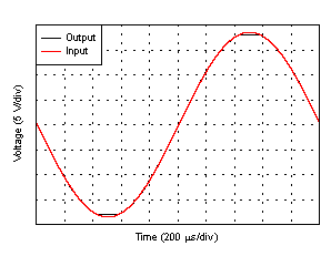
The OPAx197 family has internal phase-reversal protection. Many op amps exhibit a phase reversal when the input is driven beyond its linear common-mode range. This condition is most often encountered in noninverting circuits when the input is driven beyond the specified common-mode voltage range, causing the output to reverse into the opposite rail. The OPAx197 is a rail-to-rail input op amp; therefore, the common-mode range can extend up to the rails. Input signals beyond the rails do not cause phase reversal; instead, the output limits into the appropriate rail. This performance is shown in Figure 45.
 Figure 45. No Phase Reversal