JAJSJ37F april 2020 – march 2023 OPA205 , OPA2205 , OPA4205
PRODMIX
- 1 特長
- 2 アプリケーション
- 3 概要
- 4 Revision History
- 5 Pin Configuration and Functions
- 6 Specifications
- 7 Parameter Measurement Information
- 8 Detailed Description
- 9 Application and Implementation
- 10Device and Documentation Support
- 11Mechanical, Packaging, and Orderable Information
パッケージ・オプション
メカニカル・データ(パッケージ|ピン)
サーマルパッド・メカニカル・データ
発注情報
5 Pin Configuration and Functions
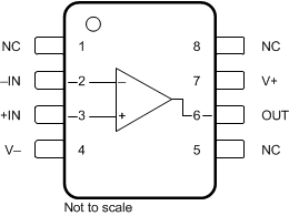
 Figure 5-1 OPA205 D Package, 8-Pin
SOIC (Top View)
Figure 5-1 OPA205 D Package, 8-Pin
SOIC (Top View)Table 5-1 Pin Functions: OPA205
| PIN | TYPE | DESCRIPTION | |
|---|---|---|---|
| NAME | NO. | ||
| +IN | 3 | Input | Noninverting input |
| –IN | 2 | Input | Inverting input |
| NC | 1, 5, 8 | — | No internal connection (can be left floating) |
| OUT | 6 | Output | Output |
| V+ | 7 | — | Positive (highest) power supply |
| V– | 4 | — | Negative (lowest) power supply |
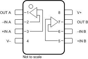
 Figure 5-2 OPA2205 DGK Package, 8-Pin
VSSOP and D Package, 8-pin SOIC (Top View)
Figure 5-2 OPA2205 DGK Package, 8-Pin
VSSOP and D Package, 8-pin SOIC (Top View)Table 5-2 Pin Functions: OPA2205
| PIN | TYPE | DESCRIPTION | |
|---|---|---|---|
| NAME | NO. | ||
| +IN A | 3 | Input | Noninverting input, channel A |
| –IN A | 2 | Input | Inverting input, channel A |
| +IN B | 5 | Input | Noninverting input, channel B |
| –IN B | 6 | Input | Inverting input, channel B |
| OUT A | 1 | Output | Output, channel A |
| OUT B | 7 | Output | Output, channel B |
| V+ | 8 | — | Positive (highest) power supply |
| V– | 4 | — | Negative (lowest) power supply |
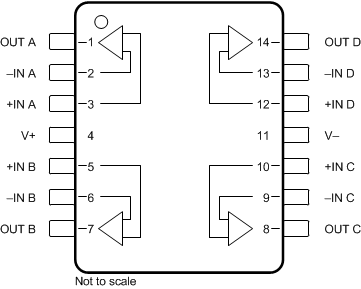
 Figure 5-3 OPA4205 PW Package, 14-Pin
TSSOP and D Package, 14-Pin SOIC (Top View)
Figure 5-3 OPA4205 PW Package, 14-Pin
TSSOP and D Package, 14-Pin SOIC (Top View)Pin Functions:
OPA4205
| PIN | TYPE | DESCRIPTION | |
|---|---|---|---|
| NAME | NO. | ||
| +IN A | 3 | Input | Noninverting input, channel A |
| +IN B | 5 | Input | Noninverting input, channel B |
| +IN C | 10 | Input | Noninverting input, channel C |
| +IN D | 12 | Input | Noninverting input, channel D |
| –IN A | 2 | Input | Inverting input, channel A |
| –IN B | 6 | Input | Inverting input, channel B |
| –IN C | 9 | Input | Inverting input, channel C |
| –IN D | 13 | Input | Inverting input, channel D |
| OUT A | 1 | Output | Output, channel A |
| OUT B | 7 | Output | Output, channel B |
| OUT C | 8 | Output | Output, channel C |
| OUT D | 14 | Output | Output, channel D |
| V+ | 4 | — | Positive (highest) power supply |
| V– | 11 | — | Negative (lowest) power supply |