JAJSF99G March 2002 – April 2018 OPA2354 , OPA354 , OPA4354
PRODUCTION DATA.
- 1 特長
- 2 アプリケーション
- 3 概要
- 4 改訂履歴
- 5 Device Comparison Table
- 6 Pin Configuration and Functions
- 7 Specifications
- 8 Detailed Description
- 9 Application and Implementation
- 10Power Supply Recommendations
- 11Layout
- 12デバイスおよびドキュメントのサポート
- 13メカニカル、パッケージ、および注文情報
パッケージ・オプション
メカニカル・データ(パッケージ|ピン)
サーマルパッド・メカニカル・データ
発注情報
11.4 PowerPAD Thermally-Enhanced Package
In addition to the regular 5-pin SOT-23 and 9-pin VSSOP packages, the single and dual versions of the OPAx354 also come in an 8-pin SOIC PowerPAD package. The 98-pin SO with PowerPAD is a standard size 8-pin SOIC package where the exposed leadframe on the bottom of the package is soldered directly to the PCB to create a low thermal resistance. This direct attachment enhances the OPAx354 power dissipation capability significantly, and eliminates the use of bulky heat sinks and slugs that are traditionally used in thermal packages. This package is easily mounted using standard PCB assembly techniques.
NOTE
Because the 8-pin HSOP PowerPAD is pin-compatible with standard 8-pin SOIC packages, the OPA354 and OPA2354 can directly replace operational amplifiers in existing sockets. Soldering the PowerPAD to the PCB is always required, even with applications that have low power dissipation. This configuration provides the necessary thermal and mechanical connection between the leadframe die pad and the PCB.
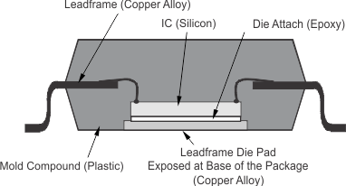
The PowerPAD package is designed so that the leadframe die pad (or thermal pad) is exposed on the bottom of the device, as shown in Figure 40. This exposed die provides an extremely low thermal resistance (RθJC) path between the die and the exterior of the package. The thermal pad on the bottom of the device can then be soldered directly to the PCB, using the PCB as a heat sink. In addition, plated-through holes (vias) provide a low thermal resistance heat flow path to the back side of the PCB.
 Figure 40. Section View of a PowerPAD Package