SBOS391B December 2007 – March 2016 OPA454
PRODUCTION DATA.
- 1 Features
- 2 Applications
- 3 Description
- 4 Revision History
- 5 Device Comparison Table
- 6 Pin Configuration and Functions
- 7 Specifications
- 8 Parameter Measurement Information
- 9 Detailed Description
- 10Application and Implementation
- 11Power Supply Recommendations
- 12Layout
- 13Device and Documentation Support
- 14Mechanical, Packaging, and Orderable Information
1 Features
2 Applications
- Test Equipment
- Avalanche Photodiode:
High-V Current Sense - Piezoelectric Cells
- Transducer Drivers
- Servo Drivers
- Audio Amplifiers
- High-Voltage Compliance Current Sources
- General High-Voltage Regulators and Power
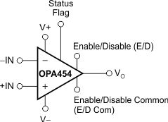
Simplified Pin Description

3 Description
The OPA454 device is a low-cost operational amplifier with high voltage (100 V) and relatively high current drive (50 mA). It is unity-gain stable and has a gain-bandwidth product of 2.5 MHz.
The OPA454 is internally protected against overtemperature conditions and current overloads. It is fully specified to perform over a wide power-supply range of ±5 V to ±50 V or on a single supply of 10 V to 100 V. The status flag is an open-drain output that allows it to be easily referenced to standard low-voltage logic circuitry. This high-voltage operational amplifier provides excellent accuracy, wide output swing, and is free from phase inversion problems that are often found in similar amplifiers.
The output can be independently disabled using the Enable or Disable Pin that has its own common return pin to allow easy interface to low-voltage logic circuitry. This disable is accomplished without disturbing the input signal path, not only saving power but also protecting the load.
Featured in a small exposed metal pad package, the OPA454 is easy to heatsink over the extended industrial temperature range, –40°C to +85°C.
Device Information(1)
| PART NUMBER | PACKAGE | BODY SIZE (NOM) |
|---|---|---|
| OPA454 | SO PowerPAD™ (8) | 4.89 mm × 3.90 mm |
- For all available packages, see the orderable addendum at the end of the data sheet.
4 Revision History
Changes from A Revision (December 2008) to B Revision
- Added Pin Functions table, ESD Ratings table, Recommended Operating Conditions table, Thermal Information table, Feature Description section, Device Functional Modes section, Application and Implementation section, Power Supply Recommendations section, Layout section, Device and Documentation Support section, and Mechanical, Packaging, and Orderable Information section Go
- Changed OPA454 Related Products table to Device Comparison tableGo
- Deleted Ordering Information tableGo
- Corrected symbol error in Absolute Maximum Ratings table; changed operating temperature specification from TJ to TA Go
- Changed Figure 29 title from THD+N vs Temperature to THD+N vs FrequencyGo
- Changed Figure 30 title from THD+N vs Temperature to THD+N vs FrequencyGo
Changes from * Revision (December 2007) to A Revision
- Deleted DDA Package from title of Figure 13Go
- Deleted DDA Package from title of Figure 14Go
- Corrected mislabeled y-axis in Figure 42Go
- Corrected mislabeled y-axis in Figure 43Go
- Corrected mislabeled y-axis in Figure 44Go
- Changed statement about thermal shutdown cycling qualification studies from 400 hours to 1000 hours in Current Limit sectionGo
- Deleted Top-Side PowerPAD Package sectionGo
- Added alternate units (.013 in, or 0.3302 mm) for measurement of recommended through-hole diameter to PowerPAD Layout Guidelines descriptionGo