JAJSRQ2A October 2023 – February 2024 OPA4990-Q1
ADVANCE INFORMATION
- 1
- 1 特長
- 2 アプリケーション
- 3 概要
- 4 Pin Configuration and Function
- 5 Specifications
- 6 Detailed Description
- 7 Application and Implementation
- 8 Device and Documentation Support
- 9 Revision History
- 10Mechanical, Packaging, and Orderable Information
パッケージ・オプション
デバイスごとのパッケージ図は、PDF版データシートをご参照ください。
メカニカル・データ(パッケージ|ピン)
- PW|14
サーマルパッド・メカニカル・データ
発注情報
6.3.4 Capacitive Load and Stability
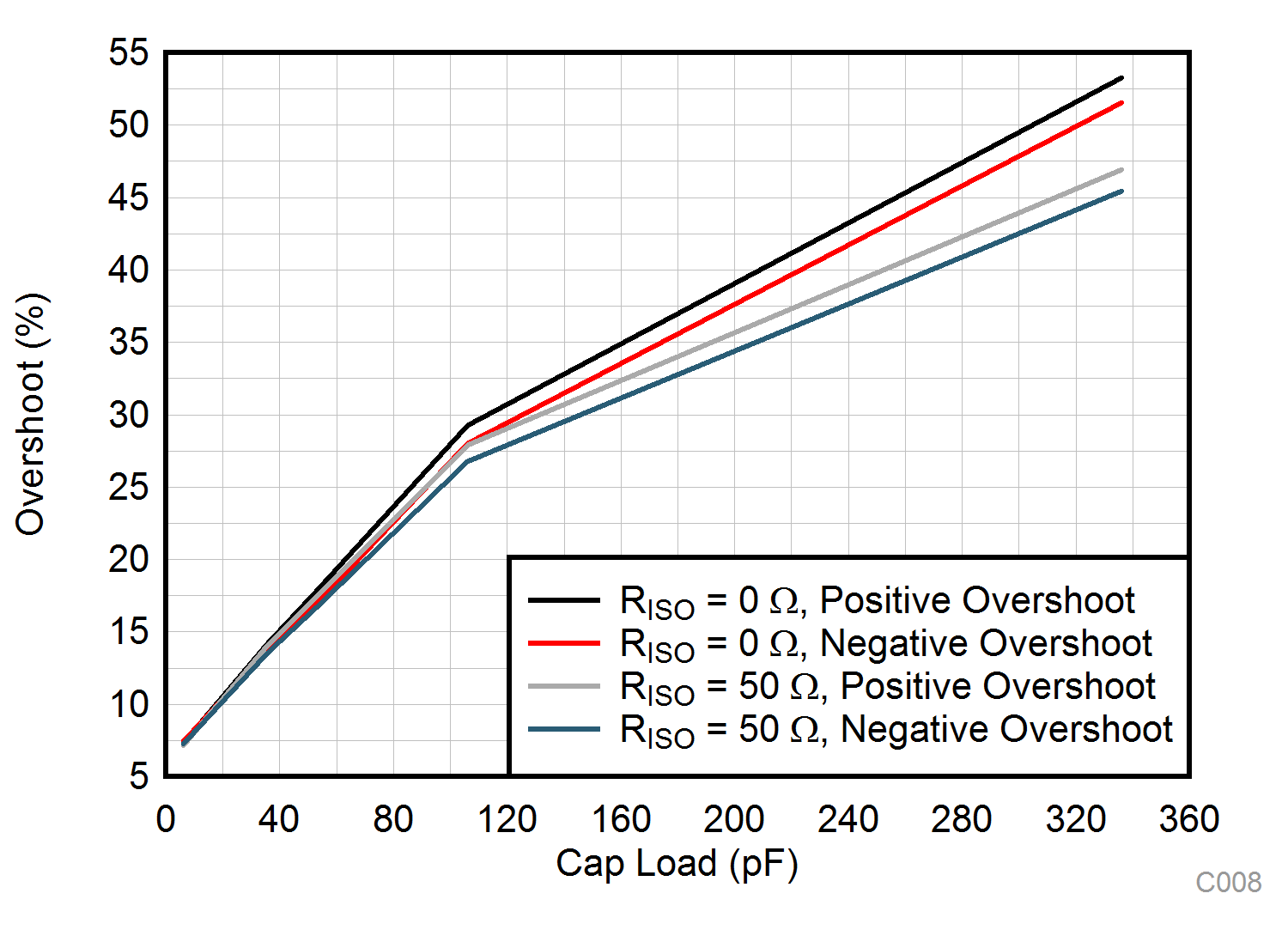
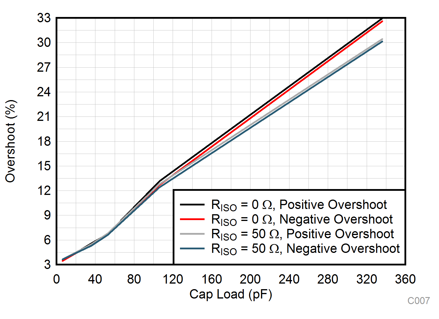
The OPAx990-Q1 features a resistive output stage capable of driving moderate capacitive loads, and by leveraging an isolation resistor, the device can easily be configured to drive large capacitive loads. As shown in Figure 6-5 and Figure 6-6, increasing the gain enhances the ability of the amplifier to drive greater capacitive loads. The particular op amp circuit configuration, layout, gain, and output loading are some of the factors to consider when establishing whether an amplifier will be stable in operation.
 Figure 6-5 Small-Signal Overshoot vs Capacitive Load (10mV Output Step, G = 1)
 Figure 6-6 Small-Signal Overshoot vs Capacitive Load (10mV Output Step, G = –1)
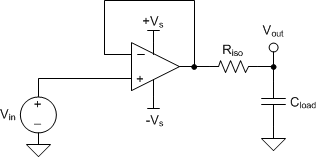
For additional drive capability in unity-gain configurations, improve capacitive load drive by inserting a small resistor, RISO, in series with the output, as shown in Figure 6-7. This resistor significantly reduces ringing and maintains DC performance for purely capacitive loads. However, if a resistive load is in parallel with the capacitive load, then a voltage divider is created, thus introducing a gain error at the output and slightly reducing the output swing. The error introduced is proportional to the ratio RISO / RL, and is generally negligible at low output levels. A high capacitive load drive makes the OPAx990-Q1 an excellent choice for applications such as reference buffers, MOSFET gate drives, and cable-shield drives. The circuit shown in Figure 6-7 uses an isolation resistor, RISO, to stabilize the output of an op amp. RISO modifies the open-loop gain of the system for increased phase margin.
 Figure 6-7 Extending Capacitive Load
Drive With the OPA990-Q1