JAJSIC3D October   1997  – December 2019 OPA548

PRODUCTION DATA.  

  1. 特長
  2. アプリケーション
    1.     概略回路図
  3. 概要
  4. 改訂履歴
  5. Pin Configuration and Functions
    1.     Pin Functions
  6. Specifications
    1. 6.1 Absolute Maximum Ratings
    2. 6.2 ESD Ratings
    3. 6.3 Recommended Operating Conditions
    4. 6.4 Thermal Information
    5. 6.5 Electrical Characteristics
    6. 6.6 Typical Characteristics
  7. Detailed Description
    1. 7.1 Overview
    2. 7.2 Functional Block Diagram
    3. 7.3 Feature Description
      1. 7.3.1 Adjustable Current Limit
      2. 7.3.2 Enable/Status (E/S) Pin
      3. 7.3.3 Thermal Shutdown Status
    4. 7.4 Device Functional Modes
      1. 7.4.1 Output Disable
  8. Application and Implementation
    1. 8.1 Application Information
    2. 8.2 Typical Applications
      1. 8.2.1 Basic Circuit Connections
        1. 8.2.1.1 Design Requirements
        2. 8.2.1.2 Detailed Design Procedure
          1. 8.2.1.2.1 Power Supply Requirements
          2. 8.2.1.2.2 Gain Setting and Input Configuration
          3. 8.2.1.2.3 Current Limit
          4. 8.2.1.2.4 Safe-Operating-Area
          5. 8.2.1.2.5 Heat Sinking
        3. 8.2.1.3 Application Curve
      2. 8.2.2 Monitoring Single- and Dual-Supplies
        1. 8.2.2.1 Design Requirements
        2. 8.2.2.2 Detailed Design Procedure
          1. 8.2.2.2.1 Output Disable and Thermal Shutdown Status
      3. 8.2.3 Programmable Power Supply
    3. 8.3 System Examples
  9. Power Supply Recommendations
    1. 9.1 Output Stage Compensation
    2. 9.2 Output Protection
  10. 10Layout
    1. 10.1 Layout Guidelines
      1. 10.1.1 Safe Operating Area
      2. 10.1.2 Amplifier Mounting
      3. 10.1.3 Power Dissipation
      4. 10.1.4 Thermal Considerations
      5. 10.1.5 Heat Sinking
        1. 10.1.5.1 Heat Sink Selection Example
    2. 10.2 Layout Example
  11. 11デバイスおよびドキュメントのサポート
    1. 11.1 デバイス・サポート
      1. 11.1.1 デベロッパー・ネットワークの製品に関する免責事項
    2. 11.2 ドキュメントのサポート
      1. 11.2.1 関連資料
    3. 11.3 ドキュメントの更新通知を受け取る方法
    4. 11.4 サポート・リソース
    5. 11.5 商標
    6. 11.6 静電気放電に関する注意事項
    7. 11.7 Glossary
  12. 12メカニカル、パッケージ、および注文情報

パッケージ・オプション

メカニカル・データ(パッケージ|ピン)
サーマルパッド・メカニカル・データ
発注情報

Programmable Power Supply

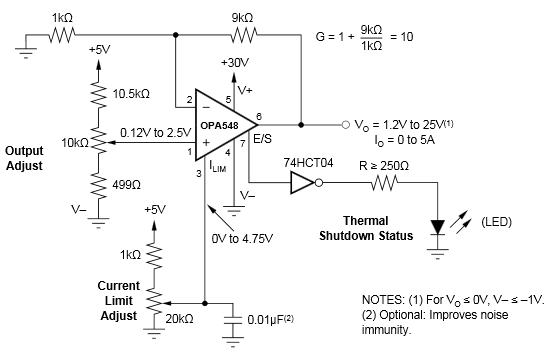
A programmable source or sink power supply can easily be built using the OPA548. Both the output voltage and output current are user-controlled. See Figure 30 for a circuit using potentiometers to adjust the output voltage and current while Figure 31 uses DACs. An LED tied to the E/S pin through a logic gate indicates if the OPA548 is in thermal shutdown.

Figure 30 illustrates how to use the OPA548 to provide an accurate voltage source with only three external resistors. First, the current limit resistor, RCL, is chosen according to the desired output current. The resulting voltage at the ILIM pin is constant and stable over temperature. This voltage, VCL, is connected to the noninverting input of the operational amplifier and used as a voltage reference, thus eliminating the need for an external reference. The feedback resistors are selected to gain VCL to the desired output voltage level.
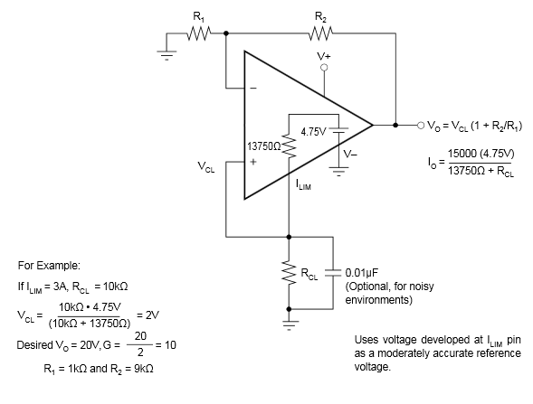
OPA548 voltagesource1.pngFigure 30. Voltage Source Schematic
OPA548 resistorcontrolled1.pngFigure 31. Resistor-Controlled Programmable Power Supply Schematic
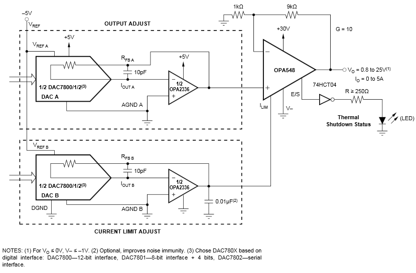
OPA548 digitallycontrolled1.pngFigure 32. Digitally-Controlled Programmable Power Supply Schematic