SBOS100B July 1999 – January 2016 OPA551 , OPA552
PRODUCTION DATA.
- 1 Features
- 2 Applications
- 3 Description
- 4 Revision History
- 5 Pin Configuration and Functions
- 6 Specifications
- 7 Detailed Description
- 8 Application and Implementation
- 9 Power Supply Recommendations
- 10Layout
- 11Device and Documentation Support
- 12Mechanical, Packaging, and Orderable Information
パッケージ・オプション
メカニカル・データ(パッケージ|ピン)
サーマルパッド・メカニカル・データ
発注情報
1 Features
- Wide Supply Range: ±4 V to ±30 V
- High Output Current: 200 mA Continuous
- Low Noise: 14 nV/√Hz
- Fully Protected:
- Thermal Shutdown
- Output Current-Limited
- Thermal Shutdown Indicator
- Wide Output Swing: 2 V from Rail
- Fast Slew Rate:
- OPA551: 15 V/µs
- OPA552: 24 V/µs
- Wide Bandwidth:
- OPA551: 3 MHz
- OPA552: 12 MHz
- Packages: PDIP-8, SOIC-8, or DDPAK/TO-263-7
2 Applications
- Telephony
- Test Equipment
- Audio Amplifiers
- Transducer Excitation
- Servo Drivers
3 Description
The OPA551x devices are low-cost operational amplifiers with high-voltage (60-V) and high-current (200-mA) capability.
The OPA551 is unity-gain stable and features high slew rate (15 V/µs) and wide bandwidth (3 MHz). The OPA552 is optimized for gains of 5 or greater, and offers higher speed with a slew rate of 24 V/µs and a bandwidth of 12 MHz. Both devices are suitable for telephony, audio, servo, and test applications.
These laser-trimmed, monolithic integrated circuits provide excellent low-level accuracy along with high output swing. High performance is maintained as the amplifier swings to its specified limits.
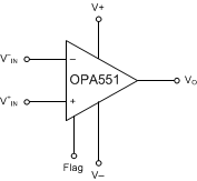
The OPA55x devices are internally protected against overtemperature conditions and current overloads. The thermal shutdown indicator flag provides a current output to alert the user when thermal shutdown has occurred.
The OPA55x devices are available in PDIP-8 and SOIC-8 packages, as well as a DDPAK-7/TO-263 surface-mount plastic power package. They are specified for operation over the extended industrial temperature range, –40°C to +125°C.
Device Information(1)
| PART NUMBER | PACKAGE | BODY SIZE (NOM) |
|---|---|---|
| OPA55x | PDIP (8) | 9.81 mm × 6.35 mm |
| SOIC (8) | 4.9 mm × 3.91 mm | |
| DDPAK/TO-263 (7) | 10.1 mm × 8.99 mm |
- For all available packages, see the orderable addendum at the end of the data sheet.
Simplified Functional Diagram
