-
OPA659 Wideband, Unity-Gain Stable, JFET-Input Operational Amplifier
- 1 Features
- 2 Applications
- 3 Description
- 4 Revision History
- 5 Related Operational Amplifier Products
- 6 Pin Configuration and Functions
- 7 Specifications
- 8 Detailed Description
- 9 Application Information
- 10Power Supply Recommendations
- 11Layout
- 12Device and Documentation Support
- 13Mechanical, Packaging, and Orderable Information
- IMPORTANT NOTICE
パッケージ・オプション
メカニカル・データ(パッケージ|ピン)
サーマルパッド・メカニカル・データ
- DRB|8
発注情報
OPA659 Wideband, Unity-Gain Stable, JFET-Input Operational Amplifier
1 Features
- High Bandwidth: 650 MHz (G = 1 V/V)
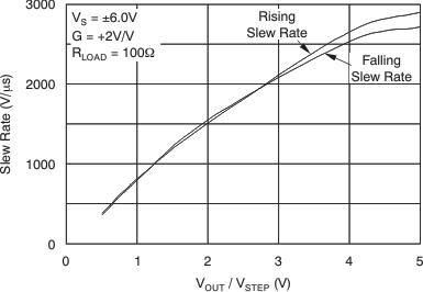
- High Slew Rate: 2550 V/μs (4-V Step)
- Excellent THD: –78 dBc at 10 MHz
- Low Input Voltage Noise: 8.9 nV/√Hz
- Fast Overdrive Recovery: 8 ns
- Fast Settling time (1% 4-V Step): 8 ns
- Low Input Offset Voltage: ±1 mV
- Low Input Bias Current: ±10 pA
- High Output Current: 70 mA
2 Applications
- High-Impedance Data Acquisition Input Amplifiers
- High-Impedance Oscilloscope Input Amplifiers
- Wideband Photodiode Transimpedance Amplifiers
- Wafer Scanning Equipment
- Optical Time-Domain Reflectometry (OTDR)
- High-Speed Time-of-Flight (TOF) Sensing
3 Description
The OPA659 combines a very wideband, unity-gain stable, voltage-feedback operational amplifier with a JFET-input stage to offer an ultra-high dynamic range amplifier for high impedance buffering in data acquisition applications such as oscilloscope front-end amplifiers and machine vision applications such as photodiode transimpedance amplifiers used in wafer inspection.
The wide 650-MHz unity-gain bandwidth is complemented by a very high 2550-V/μs slew rate.
The high input impedance and low bias current provided by the JFET input are supported by the low 8.9-nV/√Hz input voltage noise to achieve a very low integrated noise in wideband photodiode transimpedance applications.
Broad transimpedance bandwidths are possible with the high 350-MHz gain bandwidth product of this device.
Where lower speed with lower quiescent current is required, consider the OPA656. Where unity-gain stability is not required, consider the OPA657.
Device Information(1)
| PART NUMBER | PACKAGE | BODY SIZE (NOM) |
|---|---|---|
| OPA659 | SOT-23 (5) | 2.90 mm × 1.60 mm |
| SON (8) | 3.00 mm × 3.00 mm |
- For all available packages, see the orderable addendum at the end of the data sheet.
Typical Application

Transimpedance Gain vs Frequency

4 Revision History
Changes from B Revision (August 2009) to C Revision
- Added ESD Ratings table, Feature Description section, Device Functional Modes, Application and Implementation section, Power Supply Recommendations section, Layout section, Device and Documentation Support section, and Mechanical, Packaging, and Orderable Information section Go
- Deleted THERMAL CHARACTERISTICS row from Electrical Characteristics Go
Changes from A Revision (March, 2009) to B Revision
- Removed lead temperature specification from Absolute Maximum Ratings tableGo
- Added DRB package to test condition for Input Offset Voltage parameter, TA = –40°C to 85°CGo
- Added performance specifications for Input Offset Voltage parameter, DBV packageGo
- Added performance specifications for Average Offset Voltage Drift parameter, DBV packageGo
- Added footnote (2) to Electrical Characteristics (VS = ±6V) tableGo
- Added paragraph (f) to the Board Layout sectionGo
Changes from * Revision (December, 2008) to A Revision
- Changed Changed ordering information for SOTS23-5 (DBV) package and added footnote; availability expected 2Q 2009 Go
5 Related Operational Amplifier Products
| DEVICE | VS (V) | BW (MHz) | SLEW RATE (V/μs) | VOLTAGE NOISE (nV/√Hz) | AMPLIFIER DESCRIPTION |
|---|---|---|---|---|---|
| OPA659 | ±6 | 350 | 2550 | 8.9 | Unity-Gain Stable FET-Input |
| OPA656 | ±5 | 230 | 290 | 7 | Unity-Gain Stable FET-Input |
| OPA657 | ±5 | 1600 | 700 | 4.8 | Gain of +7 stable FET Input |
| LMH6629 | 5 | 4000 | 1600 | 0.69 | Gain of +10 stable Bipolar Input |
| THS4631 | ±15 | 210 | 1000 | 7 | Unity-Gain Stable FET-Input |
| OPA857 | 5 | 4750 | 220 | — | Programmable Gain (5 kΩ / 20 kΩ) Transimpedance Amplifier |
6 Pin Configuration and Functions


Pin Functions
| PIN | TYPE | DESCRIPTION | ||
|---|---|---|---|---|
| NAME | SOIC | SOT-23 | ||
| NC | 1 | — | — | No Connection |
| 5 | ||||
| 8 | ||||
| VIN– | 2 | 4 | I | Inverting Input |
| VIN+ | 3 | 3 | I | Noninverting Input |
| VOUT | 6 | 1 | O | Output of amplifier |
| –VS | 4 | 2 | POW | Negative Power Supply |
| +VS | 7 | 5 | POW | Positive Power Supply |
7 Specifications
7.1 Absolute Maximum Ratings
Over operating free-air temperature range (unless otherwise noted).| MIN | MAX | UNIT | ||
|---|---|---|---|---|
| Power Supply Voltage VS+ to VS– | ±6.5 | V | ||
| Input Voltage | ±VS | V | ||
| Input Current | 100 | mA | ||
| Output Current | 100 | mA | ||
| Continuous Power Dissipation | See Thermal Information | |||
| Operating Free Air Temperature, TA | –40 | 85 | °C | |
| Maximum Junction Temperature, TJ | 150 | °C | ||
| Maximum Junction Temperature, TJ (continuous operation for long term reliability) | 125 | °C | ||
| Storage Temperature, Tstg | –65 | 150 | °C | |
7.2 ESD Ratings
| VALUE | UNIT | |||
|---|---|---|---|---|
| V(ESD) | Electrostatic discharge | Human-body model (HBM), per ANSI/ESDA/JEDEC JS-001(1) | ±4000 | V |
| Charged-device model (CDM), per JEDEC specification JESD22-C101(2) | ±1000 | |||
| Machine model (MM) | ±200 | |||
7.3 Recommended Operating Conditions
over operating free-air temperature range (unless otherwise noted)| MIN | NOM | MAX | UNIT | ||
|---|---|---|---|---|---|
| VS | Total supply voltage | 7 | 12 | 13 | V |
| TA | Ambient temperature | –40 | 25 | 85 | °C |
7.4 Thermal Information
| THERMAL METRIC(1) | OPA659 | UNIT | ||
|---|---|---|---|---|
| DRB (VSON) | DRV (SOT23) | |||
| 8 PINS | 5 PINS | |||
| RθJA | Junction-to-ambient thermal resistance | 56.3 | 209 | °C/W |
| RθJC(top) | Junction-to-case (top) thermal resistance | 63.7 | 124 | °C/W |
| RθJB | Junction-to-board thermal resistance | 31.9 | 38.1 | °C/W |
| ψJT | Junction-to-top characterization parameter | 3.2 | 15 | °C/W |
| ψJB | Junction-to-board characterization parameter | 32.1 | 37.2 | °C/W |
| RθJC(bot) | Junction-to-case (bottom) thermal resistance | 15.3 | — | °C/W |
7.5 Electrical Characteristics
At RF = 0 Ω, G = 1 V/V, and RL = 100 Ω, TA = 25°C, VS = ±6 V unless otherwise noted.| PARAMETER | TEST CONDITIONS | TEST LEVEL(1) | MIN | TYP | MAX | UNIT | |||
|---|---|---|---|---|---|---|---|---|---|
| AC PERFORMANCE | |||||||||
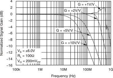
| Small-Signal Bandwidth | VO = 200 mVPP, G = 1 V/V | C | 650 | MHz | |||||
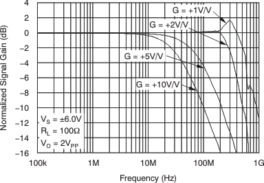
| VO = 200 mVPP, G = 2 V/V | C | 335 | MHz | ||||||
| VO = 200 mVPP, G = 5 V/V | C | 75 | MHz | ||||||
| VO = 200 mVPP, G = 10 V/V | C | 35 | MHz | ||||||
| Gain Bandwidth Product | G > 10 V/V | C | 350 | MHz | |||||
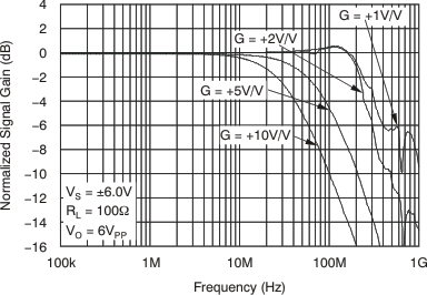
| Bandwidth for 0.1dB Flatness | G = 2 V/V, VO = 2VPP | C | 55 | MHz | |||||
| Large-Signal Bandwidth | VO = 2 VPP, G = 1 V/V | B | 575 | MHz | |||||
| Slew Rate | VO = 4-V Step, G = 1 V/V | B | 2550 | V/μs | |||||
| Rise and Fall Time | VO = 4-V Step, G = 1 V/V | C | 1.3 | ns | |||||
| Settling Time to 1% | VO = 4-V Step, G = 1 V/V | C | 8 | ns | |||||
| Pulse Response Overshoot | VO = 4-V Step, G = 1 V/V | C | 12% | ||||||
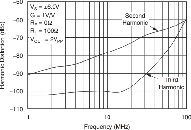
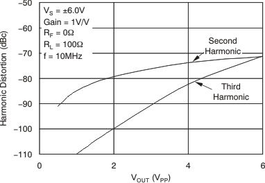
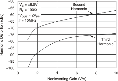
| Harmonic Distortion, 2nd harmonic | VO = 2 VPP, G = 1 V/V, f = 10 MHz | C | –79 | dBc | |||||
| Harmonic Distortion, 3rd harmonic | VO = 2 VPP, G = 1 V/V, f = 10 MHz | C | –100 | dBc | |||||
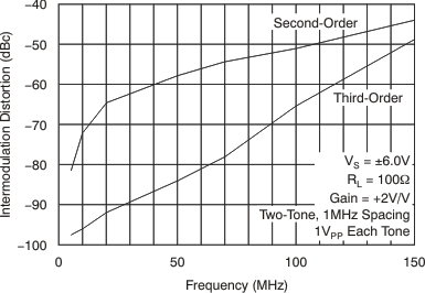
| Intermodulation Distortion, 2nd intermodulation | VO= 2 VPP Envelope (each tone 1 VPP), G = 2 V/V, f1 = 10 MHz, f2 = 11 MHz |
C | –72 | dBc | |||||
| Intermodulation Distortion, 3rd intermodulation | VO= 2 VPP Envelope (each tone 1 VPP), G = 2 V/V, f1 = 10 MHz, f2 = 11 MHz |
C | –96 | dBc | |||||
| Input Voltage Noise | f > 100 kHz | C | 8.9 | nV/√Hz | |||||
| Input Current Noise | f < 10 MHz | C | 1.8 | fA/√Hz | |||||
| DC PERFORMANCE | |||||||||
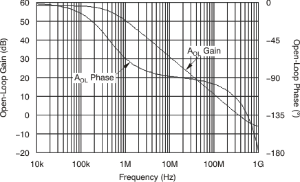
| Open-Loop Voltage Gain (AOL) | TA = 25°C, VCM = 0 V, RL = 100 Ω | A | 52 | 58 | dB | ||||
| TA = –40°C to 85°C, VCM = 0 V, RL = 100 Ω | B | 49 | 55 | dB | |||||
| Input Offset Voltage | TA = 25°C, VCM = 0 V | A | ±1 | ±5 | mV | ||||
| TA = –40°C to 85°C, VCM = 0 V DRB package | DRB package | B | ±1.5 | ±7.6 | mV | ||||
| DBV package | B | ±1.5 | ±8.9 | mV | |||||
| Average input-offset voltage drift(2) | TA = –40°C to 85°C, VCM = 0 V | DRB package | B | ±10 | ±40 | μV/°C | |||
| DBV package | B | ±10 | ±60 | μV/°C | |||||
| Input Bias Current | TA = 25°C, VCM = 0 V | A | ±10 | ±50 | pA | ||||
| TA = 0°C to 70°C, VCM = 0 V | B | ±240 | ±1200 | pA | |||||
| TA = –40°C to 85°C, VCM = 0 V | B | ±640 | ±3200 | pA | |||||
| Average input bias current drift | TA = 0°C to 70°C, VCM = 0 V | B | ±5 | ±26 | pA/°C | ||||
| TA = –40°C to 85°C, VCM = 0 V | B | ±7 | ±34 | pA/°C | |||||
| Input Offset Current | TA = 25°C, VCM = 0 V | A | ±5 | ±25 | pA | ||||
| TA = 0°C to 70°C, VCM = 0 V | B | ±120 | ±600 | pA | |||||
| TA = –40°C to 85°C, VCM = 0 V | B | ±320 | ±1600 | pA | |||||
| INPUT | |||||||||
| Common-Mode Input Range(3) | TA = 25°C | A | ±3 | ±3.5 | V | ||||
| TA = –40°C to 85°C | B | ±2.87 | ±3.37 | V | |||||
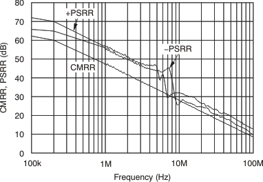
| Common-Mode Rejection Ratio | TA = 25°C, VCM = ±0.5 V | A | 68 | 70 | dB | ||||
| TA = –40°C to 85°C, VCM = ±0.5 V | B | 64 | 66 | dB | |||||
| Input Impedance | |||||||||
| Input impedance, differential | C | 1012 ∥ 1 | Ω ∥ pF | ||||||
| Input impedance, common-mode | C | 1012 ∥ 2.5 | Ω ∥ pF | ||||||
| OUTPUT | |||||||||
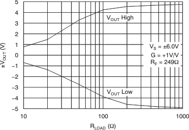
| Output Voltage Swing | TA = 25°C, | No Load | A | ±4.6 | ±4.8 | V | |||
| RL = 100 Ω | A | ±3.8 | ±4 | V | |||||
| TA = –40°C to 85°C | No Load | B | ±4.45 | ±4.65 | V | ||||
| RL = 100 Ω | B | ±3.65 | ±3.85 | V | |||||
| Output Current, Sourcing, Sinking | TA = 25°C | A | ±60 | ±70 | mA | ||||
| TA = –40°C to 85°C | B | ±56 | ±65 | mA | |||||
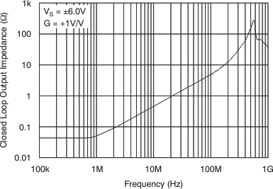
| Closed-Loop Output Impedance | G = 1 V/V, f = 100 kHz | C | 0.04 | Ω | |||||
| POWER SUPPLY | |||||||||
| Operating Voltage | B | ±3.5 | ±6 | ±6.5 | V | ||||
| Quiescent Current | TA = 25°C | A | 30.5 | 32 | 33.5 | mA | |||
| TA = –40°C to 85°C | B | 28.3 | 35.7 | mA | |||||
| Power-Supply Rejection Ratio (PSRR) | TA = 25°C, VS = ±5.5 V to ±6.5 V | A | 58 | 62 | dB | ||||
| TA = –40°C to 85°C, VS = ±5.5 V to ±6.5 V | A | 56 | 60 | dB | |||||
7.6 Typical Characteristics
At VS = ±6 V, RF = 0 Ω, G = 1 V/V, and RL = 100 Ω, unless otherwise noted.Table 1. Table of Graphs
| TITLE | FIGURE | |
|---|---|---|
| Noninverting Small-Signal Frequency Response | VO = 200 mVPP | Figure 1 |
| Noninverting Large-Signal Frequency Response | VO = 2 VPP | Figure 2 |
| Noninverting Large-Signal Frequency Response | VO = 6 VPP | Figure 3 |
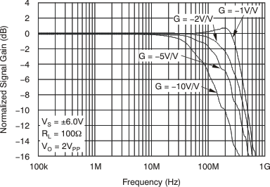
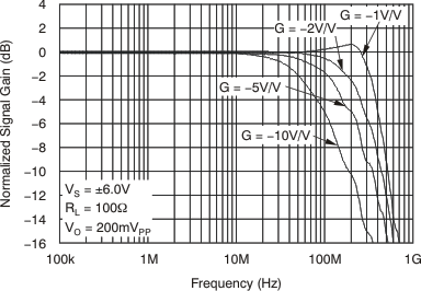
| Inverting Small-Signal Frequency Response | VO = 200 mVPP | Figure 4 |
| Inverting Large-Signal Frequency Response | VO = 2 VPP | Figure 5 |
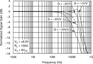
| Inverting Large-Signal Frequency Response | VO = 6 VPP | Figure 6 |
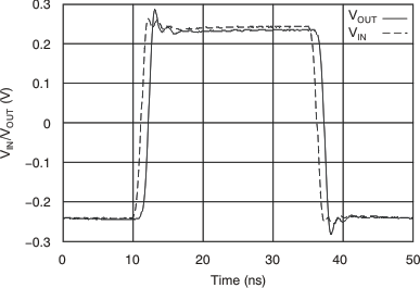
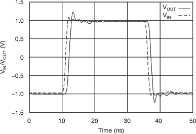
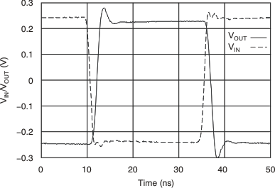
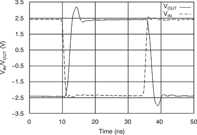
| Noninverting Transient Response | 0.5-V Step | Figure 7 |
| Noninverting Transient Response | 2-V Step | Figure 8 |
| Noninverting Transient Response | 5-V Step | Figure 9 |
| Inverting Transient Response | 0.5-V Step | Figure 10 |
| Inverting Transient Response | 2-V Step | Figure 11 |
| Inverting Transient Response | 5-V Step | Figure 12 |
| Harmonic Distortion vs Frequency | Figure 13 | |
| Harmonic Distortion vs Noninverting Gain | Figure 14 | |
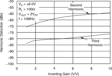
| Harmonic Distortion vs Inverting Gain | Figure 15 | |
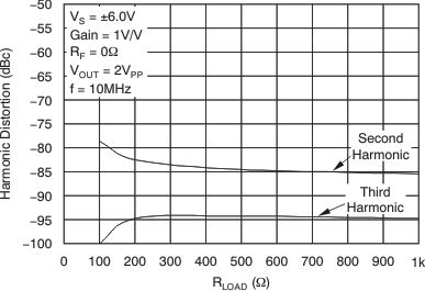
| Harmonic Distortion vs Load Resistance | Figure 16 | |
| Harmonic Distortion vs Output Voltage | Figure 17 | |
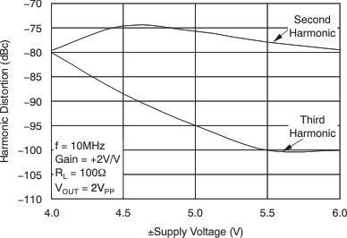
| Harmonic Distortion vs ±Supply Voltage | Figure 18 | |
| Two-Tone, Second- and Third-Order Intermodulation Distortion vs Frequency | Figure 19 | |
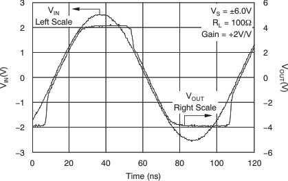
| Overdrive Recovery | Gain = 2 V/V | Figure 20 |
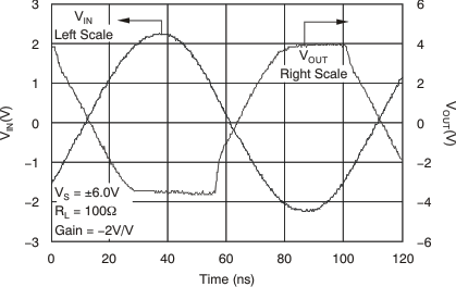
| Overdrive Recovery | Gain = –2 V/V | Figure 21 |
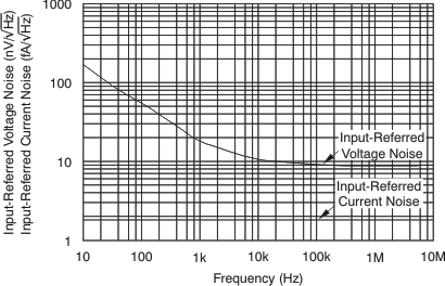
| Input-Referred Voltage Spectral Noise Density | Figure 22 | |
| Common-Mode Rejection Ratio and Power-Supply Rejection Ratio vs Frequency | Figure 23 | |
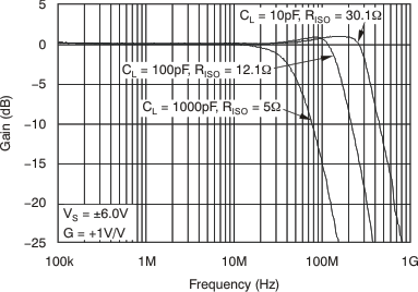
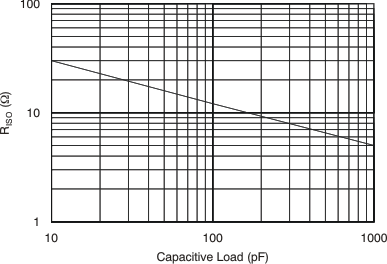
| Recommended RISO vs Capacitive Load | Figure 24 | |
| Frequency Response vs Capacitive Load | Figure 25 | |
| Open-Loop Gain and Phase | Figure 26 | |
| Closed-Loop Output Impedance vs Frequency | Figure 27 | |
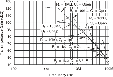
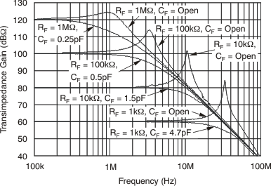
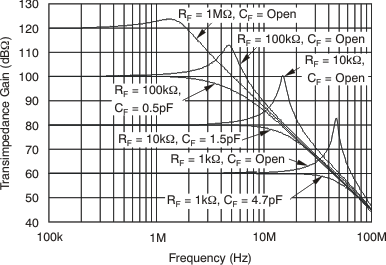
| Transimpedance Gain vs Frequency | CD = 10 pF | Figure 28 |
| Transimpedance Gain vs Frequency | CD = 22 pF | Figure 29 |
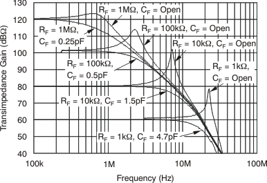
| Transimpedance Gain vs Frequency | CD = 47 pF | Figure 30 |
| Transimpedance Gain vs Frequency | CD = 100 pF | Figure 31 |
| Maximum/Minimum ±VOUT vs RLOAD | Figure 32 | |
| Slew Rate vs VOUT Step | Figure 33 | |
(VO = 2 VPP)
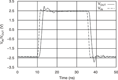
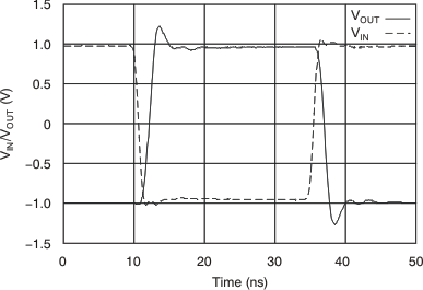
(RLOAD = 1 kΩ)
(CD = 100 pF)
(VO = 200 mVPP)
(VO = 6 VPP)
10 MHz
10 MHz
(RLOAD = 1 kΩ)
