JAJSVI0H December 2001 – October 2024 OPA690
PRODUCTION DATA
- 1
- 1 特長
- 2 アプリケーション
- 3 概要
- 4 Device Comparison Table
- 5 Pin Configuration and Functions
-
6 Specifications
- 6.1 Absolute Maximum Ratings
- 6.2 ESD Ratings
- 6.3 Recommended Operating Conditions
- 6.4 Thermal Information
- 6.5 Electrical Characteristics OPA690IDBV, VS = ±5 V
- 6.6 Electrical Characteristics OPA690IDBV, VS = 5 V
- 6.7 Electrical Characteristics OPA690ID, VS = ±5 V
- 6.8 Electrical Characteristics OPA690ID, VS = 5 V
- 6.9 Typical Characteristics: OPA690IDBV, VS = ±5V
- 6.10 Typical Characteristics: OPA690IDBV, VS = 5V
- 6.11 Typical Characteristics: OPA690ID, VS = ±5V
- 6.12 Typical Characteristics: OPA690ID, VS = 5V
- 7 Detailed Description
- 8 Application and Implementation
- 9 Device and Documentation Support
- 10Revision History
- 11Mechanical, Packaging, and Orderable Information
パッケージ・オプション
メカニカル・データ(パッケージ|ピン)
サーマルパッド・メカニカル・データ
発注情報
8.1.7 Noise Performance
High slew rate, unity-gain stable, voltage-feedback op amps usually achieve a slew rate at the expense of a higher input noise voltage. The 5.5-nV/√Hz input voltage noise for the OPA690 is, however, much lower than comparable amplifiers. The input-referred voltage noise, and the two input-referred current noise terms, combine to give low output noise under a wide variety of operating conditions. Figure 8-4 shows the op amp noise analysis model with all the noise terms included. In this model, all noise terms are taken to be noise voltage or current density terms in either nV/√Hz or pA/√Hz.
 Figure 8-4 Op Amp
Noise Analysis Model
Figure 8-4 Op Amp
Noise Analysis ModelThe total output spot noise voltage can be computed as the square root of the sum of all squared output noise voltage contributors. Equation 1 shows the general form for the output noise voltage using the terms shown in Figure 8-4.

Dividing this expression by the noise gain [NG = (1 + RF/RG)] gives the equivalent input-referred spot noise voltage at the noninverting input, as shown in Equation 2.
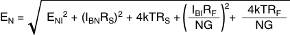
Evaluating these two equations for the OPA690 circuit and component values (see Figure 7-1) gives a total output spot noise voltage of 12.3 nV/√Hz and a total equivalent input spot noise voltage of 6.1 nV/√Hz. This is including the noise added by the bias current cancellation resistor (175 Ω) on the noninverting input. This total input-referred spot noise voltage is only slightly higher than the 5.5-nV/√Hz specification for the op amp voltage noise alone. This is the case as long as the impedances appearing at each op amp input are limited to the previously recommend maximum value of 300 Ω. Keeping both (RF || RG) and the noninverting input source impedance less than 300 Ω satisfies both noise and frequency response flatness considerations. Because the resistor-induced noise is relatively negligible, additional capacitive decoupling across the bias current cancellation resistor (RB) for the inverting op amp configuration of Figure 8-1 is not required.