JAJSVI0H December 2001 – October 2024 OPA690
PRODUCTION DATA
- 1
- 1 特長
- 2 アプリケーション
- 3 概要
- 4 Device Comparison Table
- 5 Pin Configuration and Functions
-
6 Specifications
- 6.1 Absolute Maximum Ratings
- 6.2 ESD Ratings
- 6.3 Recommended Operating Conditions
- 6.4 Thermal Information
- 6.5 Electrical Characteristics OPA690IDBV, VS = ±5 V
- 6.6 Electrical Characteristics OPA690IDBV, VS = 5 V
- 6.7 Electrical Characteristics OPA690ID, VS = ±5 V
- 6.8 Electrical Characteristics OPA690ID, VS = 5 V
- 6.9 Typical Characteristics: OPA690IDBV, VS = ±5V
- 6.10 Typical Characteristics: OPA690IDBV, VS = 5V
- 6.11 Typical Characteristics: OPA690ID, VS = ±5V
- 6.12 Typical Characteristics: OPA690ID, VS = 5V
- 7 Detailed Description
- 8 Application and Implementation
- 9 Device and Documentation Support
- 10Revision History
- 11Mechanical, Packaging, and Orderable Information
パッケージ・オプション
メカニカル・データ(パッケージ|ピン)
サーマルパッド・メカニカル・データ
発注情報
7.4.1 Disable Operation
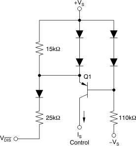
The OPA690 provides an optional disable feature that can be used either to reduce system power or to implement a simple channel multiplexing operation. If the DIS control pin is unconnected, the OPA690 operates normally. To disable, assert the control pin low. Figure 7-4 shows a simplified internal circuit for the disable control feature.
 Figure 7-4 Simplified Disable Control Circuit
The supply current in the disable mode are only those required to operate the circuit of Figure 7-4. Additional circuitry enables a faster turn-on time than turn-off time (make-before-break).
When disabled, the output and input nodes go to a high-impedance state. If the OPA690 is operating at a gain of 1, the device shows a very high impedance at the output and exceptional signal isolation. If operating at a gain greater than 1, the total feedback network resistance (RF + RG) appears as the impedance looking back into the output, but the circuit still shows very high forward and reverse isolation. If configured as an inverting amplifier, the input and output is connected through the feedback network resistance (RF + RG) and the isolation is very poor as a result.