JAJSVI0H December 2001 – October 2024 OPA690
PRODUCTION DATA
- 1
- 1 特長
- 2 アプリケーション
- 3 概要
- 4 Device Comparison Table
- 5 Pin Configuration and Functions
-
6 Specifications
- 6.1 Absolute Maximum Ratings
- 6.2 ESD Ratings
- 6.3 Recommended Operating Conditions
- 6.4 Thermal Information
- 6.5 Electrical Characteristics OPA690IDBV, VS = ±5 V
- 6.6 Electrical Characteristics OPA690IDBV, VS = 5 V
- 6.7 Electrical Characteristics OPA690ID, VS = ±5 V
- 6.8 Electrical Characteristics OPA690ID, VS = 5 V
- 6.9 Typical Characteristics: OPA690IDBV, VS = ±5V
- 6.10 Typical Characteristics: OPA690IDBV, VS = 5V
- 6.11 Typical Characteristics: OPA690ID, VS = ±5V
- 6.12 Typical Characteristics: OPA690ID, VS = 5V
- 7 Detailed Description
- 8 Application and Implementation
- 9 Device and Documentation Support
- 10Revision History
- 11Mechanical, Packaging, and Orderable Information
パッケージ・オプション
メカニカル・データ(パッケージ|ピン)
サーマルパッド・メカニカル・データ
発注情報
8.1.5 Driving Capacitive Loads
One of the most demanding and yet very common load conditions for an op amp is capacitive loading. Often, the capacitive load is the input of an ADC—including additional external capacitance that can be recommended to improve ADC linearity. A high-speed, high open-loop gain amplifier like the OPA690 can be very susceptible to decreased stability and closed-loop response peaking when a capacitive load is placed directly on the output pin. When the amplifier open-loop output resistance is considered, this capacitive load introduces an additional pole in the signal path that can decrease the phase margin. Several external solutions to this problem have been suggested. When the primary considerations are frequency response flatness, pulse response fidelity, and distortion, the simplest and most effective solution is to isolate the capacitive load from the feedback loop by inserting a series-isolation resistor between the amplifier output and the capacitive load. This configuration does not eliminate the pole from the loop response, but rather shifts the pole and adds a zero at a higher frequency. The additional zero acts to cancel the phase lag from the capacitive load pole, thus increasing the phase margin and improving stability.
The typical characteristics show the recommended RS versus capacitive load (Figure 6-51 for ±5 V and Figure 6-66 for 5 V), and the resulting frequency response at the load. Parasitic capacitive loads greater than 2 pF can begin to degrade the performance of the OPA690. Long PCB traces, unmatched cables, and connections to multiple devices can easily exceed this value. Always consider this effect carefully, and add the recommended series resistor as close as possible to the OPA690 output pin (see Section 8.4.1).
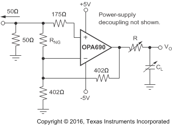
The criterion for setting this RS resistor is a maximum bandwidth, flat frequency response at the load. For the OPA690 operating in a gain of 2, the frequency response at the output pin is already slightly peaked without the capacitive load requiring relatively high values of RS to flatten the response at the load. Increasing the noise gain reduces the peaking as described previously. The circuit of Figure 8-2 demonstrates this technique, allowing lower values of RS to be used for a given capacitive load.
 Figure 8-2 Capacitive Load Driving With Noise Gain Tuning
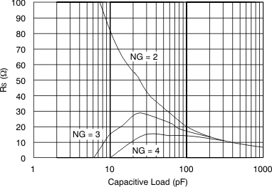
This gain of 2 V/V circuit includes a noise gain tuning resistor across the two inputs to increase the noise gain, increasing the unloaded phase margin for the op amp. Although this technique reduces the required RS resistor for a given capacitive load, this technique does increase the noise at the output. This technique also decreases the loop gain, slightly decreasing the distortion performance. If, however, the dominant distortion mechanism arises from a high RS value, significant dynamic range improvement can be achieved using this technique. Figure 8-3 shows the required RS versus CLOAD parametric on noise gain using this technique. This is the circuit of Figure 8-2 with RNG adjusted to increase the noise gain (increasing the phase margin) then sweeping CLOAD and finding the required RS to get a flat frequency response. This plot also gives the required RS versus CLOAD for the OPA690 operated at higher signal gains.
 Figure 8-3 Required
RS vs Noise Gain