JAJSP64J December 2003 – March 2025 OPA695
PRODUCTION DATA
- 1
- 1 特長
- 2 アプリケーション
- 3 説明
- 4 ピン構成および機能
-
5 仕様
- 5.1 絶対最大定格
- 5.2 ESD 定格
- 5.3 推奨動作条件
- 5.4 熱に関する情報
- 5.5 電気的特性 VS = ±5V、OPA695ID、OPA695IDBV、OPA695DSG
- 5.6 電気的特性 VS = 5V、OPA695ID、OPA695IDBV、OPA695DSG
- 5.7 電気的特性:VS = ±5V、OPA695IDGK
- 5.8 電気的特性 VS = 5V、OPA695IDGK
- 5.9 代表的特性:VS = ±5V、OPA695IDBV、OPA695ID、OPA695DSG
- 5.10 代表的特性:VS = 5V、OPA695IDBV、OPA695ID、OPA695DSG
- 5.11 代表的特性:VS = ±5V、OPA695IDGK
- 5.12 代表的特性:VS = 5V、OPA695IDGK
- 6 詳細説明
- 7 アプリケーションと実装
- 8 デバイスおよびドキュメントのサポート
- 9 改訂履歴
- 10メカニカル、パッケージ、および注文情報
パッケージ・オプション
デバイスごとのパッケージ図は、PDF版データシートをご参照ください。
メカニカル・データ(パッケージ|ピン)
- D|8
- DBV|6
- DGK|8
- DSG|8
サーマルパッド・メカニカル・データ
- DSG|8
発注情報
7.1.1.5 ノイズ性能
OPA695 は、電圧ノイズ項と電流ノイズ項の間のバランスが優れているため、低出力ノイズを実現します。反転電流ノイズ (22pA/√Hz) は、他のほとんどの電流帰還型オペアンプよりも低く、入力電圧ノイズ (1.8nV/√Hz) はユニティゲイン安定、広帯域、電圧帰還型オペアンプよりも低くなっています。低い入力電圧ノイズは、より高い非反転入力電流ノイズ (18pA/√Hz) と引き換えにして、実現しました。非反転ノードからの AC ソース インピーダンスが 50Ω 未満である限り、この電流ノイズは合計出力ノイズに大きく影響しません。オペアンプの入力電圧ノイズと 2 つの入力電流ノイズ項を組み合わせることで、さまざまな動作条件下で低出力ノイズが得られます。図 7-4 には、すべてのノイズ項を含めたオペアンプのノイズ解析モデルが示されています。このモデルでは、すべてのノイズ項は、nV/√Hz か pA/√Hz のいずれかのノイズ電圧または電流密度項として扱われます。
 図 7-4 オペアンプのノイズ指数解析モデル
合計出力スポット ノイズ電圧は、寄与するすべての出力ノイズ電圧の 2 乗和の平方根として計算できます。式 1 は、図 7-8 に示されている項を使用した出力ノイズ電圧の一般的な式となります。

この式をノイズ ゲイン (NG = (1 + RF/ RG)) で割ると、式 2 に示すように、非反転入力における等価入力換算スポット ノイズ電圧が得られます
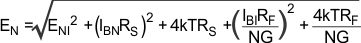
図 6-1に示すこれら 2 つの式をの OPA695 回路と部品の値で評価すると、合計出力スポット ノイズ電圧は 18.7nV/√Hz、合計等価入力スポット ノイズ電圧は 2.3nV/√Hz となります。この合計入力換算スポット ノイズ電圧は、オペアンプの電圧ノイズのみの仕様である 1.8-nV/√Hz よりも高くなります。これは、反転電流ノイズと帰還抵抗によって出力に追加されるノイズによるものです。高ゲイン構成で帰還抵抗を小さくすると (前述のように)式 2で与えられる総合入力換算電圧ノイズは、オペアンプの 1.8nV/√Hz に近付きます。たとえば、ゲイン +20 にすると (RF = 200Ω を使用して)、合計入力換算ノイズは 2.0nV/√Hz になります。
オペアンプのノイズ計算の詳細については、www.ti.com から入手可能な『高速オペアンプのノイズ解析』アプリケーション ノートを参照してください。