JAJSP64I December 2003 – October 2024 OPA695
PRODUCTION DATA
- 1
- 1 特長
- 2 アプリケーション
- 3 概要
- 4 Pin Configuration and Functions
-
5 Specifications
- 5.1 Absolute Maximum Ratings
- 5.2 ESD Ratings
- 5.3 Recommended Operating Conditions
- 5.4 Thermal Information
- 5.5 Electrical Characteristics VS = ±5 V, OPA695ID, OPA695IDBV
- 5.6 Electrical Characteristics VS = 5 V, OPA695ID, OPA695IDBV
- 5.7 Electrical Characteristics VS = ±5 V, OPA695IDGK
- 5.8 Electrical Characteristics VS = 5 V, OPA695IDGK
- 5.9 Typical Characteristics: VS = ±5 V, OPA695IDBV, OPA695ID
- 5.10 Typical Characteristics: VS = 5 V, OPA695IDBV, OPA695ID
- 5.11 Typical Characteristics: VS = ±5 V, OPA695IDGK
- 5.12 Typical Characteristics: VS = 5 V, OPA695IDGK
- 6 Detailed Description
- 7 Application and Implementation
- 8 Device and Documentation Support
- 9 Revision History
- 10Mechanical, Packaging, and Orderable Information
パッケージ・オプション
メカニカル・データ(パッケージ|ピン)
サーマルパッド・メカニカル・データ
発注情報
4 Pin Configuration and Functions
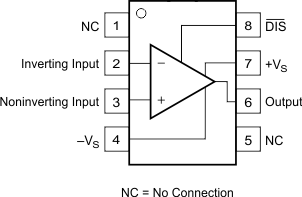
 Figure 4-1 D Package, 8-Pin SOIC, and
DGK Package, 8-Pin VSSOP (Top View)
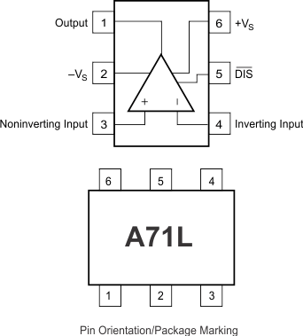
 Figure 4-2 DBV Package, 6-Pin SOT-23
(Top View)
Figure 4-2 DBV Package, 6-Pin SOT-23
(Top View)Table 4-1 Pin Functions
| PIN | TYPE(1) | DESCRIPTION | ||
|---|---|---|---|---|
| NAME | NO. | |||
| D (SOIC), DGK (VSSOP) |
DBV (SOT-23) | |||
| DIS | 8 | 5 | I | Not disable (enable) |
| Inverting input | 2 | 4 | I | Inverting input |
| NC | 1, 5 | — | — | Not connected |
| Noninverting input | 3 | 3 | I | Noninverting input |
| Output | 6 | 1 | O | Output |
| –VS | 4 | 2 | P | Negative supply |
| +VS | 7 | 6 | P | Positive supply |
(1) I = input, O = output, P = power