JAJSHS6E August 2019 – August 2024 OPA810
PRODUCTION DATA
- 1
- 1 特長
- 2 アプリケーション
- 3 概要
- 4 Device Comparison Table
- 5 Pin Configuration and Functions
-
6 Specifications
- 6.1 Absolute Maximum Ratings
- 6.2 ESD Ratings
- 6.3 Recommended Operating Conditions
- 6.4 Thermal Information
- 6.5 Electrical Characteristics: 10 V
- 6.6 Electrical Characteristics: 24 V
- 6.7 Electrical Characteristics: 5 V
- 6.8 Typical Characteristics: VS = 10 V
- 6.9 Typical Characteristics: VS = 24 V
- 6.10 Typical Characteristics: VS = 5 V
- 6.11 Typical Characteristics: ±2.375-V to ±12-V Split Supply
- 7 Detailed Description
- 8 Application and Implementation
- 9 Device and Documentation Support
- 10Revision History
- 11Mechanical, Packaging, and Orderable Information
パッケージ・オプション
デバイスごとのパッケージ図は、PDF版データシートをご参照ください。
メカニカル・データ(パッケージ|ピン)
- D|8
- DBV|5
- DCK|5
サーマルパッド・メカニカル・データ
発注情報
8.2.3 Multichannel Sensor Interface
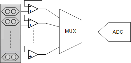
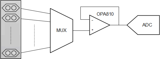
High-Z input amplifiers are particularly useful when interfaced with sensors that have relatively high output impedance. Such multichannel systems usually interface these sensors with the signal chain through a multiplexer. Figure 8-16 shows one such implementation using an amplifier for the interface with each sensor, and driving into an ADC through a multiplexer. An alternate circuit, shown in Figure 8-17, can use a single higher GBWP and fast-settling amplifier at the output of the multiplexer. This architecture gives rise to large signal transients when switching between channels, where the settling performance of the amplifier and maximum allowed differential input voltage limits signal chain performance and amplifier reliability, respectively.
 Figure 8-16 Multichannel Sensor Interface Using Multiple Amplifiers
 Figure 8-17 Multichannel Sensor Interface Using a Single Higher GBWP Amplifier
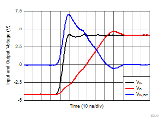
Figure 8-18 shows the output voltage and input differential voltage when a 8-V step is applied at the noninverting terminal of the OPA810 configured as a unity-gain buffer of Figure 8-17.
 Figure 8-18 Large-Signal Transient Response Using the OPA810
Because of the fast input transient, the amplifier is slew-limited and the inputs cease to track each other (a maximum VIN,Diff of 7 V is shown in Figure 8-18) until the output reaches the final value and the negative feedback loop is closed. For standard amplifiers with a 0.7-V to 1.5-V maximum VIN,Diff rating, current-limiting resistors must be used in series with the input pins to protect the device from irreversible damage, which also limits the device frequency response. The OPA810 has built-in input clamps that allow the application of as much as 7 V of VIN,Diff, with no external resistors required and no damage to the device or a shift in performance specifications. Such an input-stage architecture, coupled with the fast settling performance, makes the OPA810 a good fit for multichannel sensor multiplexed systems.