JAJSJX2 October 2020 OPA856
PRODUCTION DATA
- 1 特長
- 2 アプリケーション
- 3 概要
- 4 Revision History
- 5 Device Comparison Table
- 6 Pin Configuration and Functions
- 7 Specifications
- 8 Detailed Description
- 9 Application and Implementation
- 10Power Supply Recommendations
- 11Layout
- 12Device and Documentation Support
- 13Mechanical, Packaging, and Orderable Information
パッケージ・オプション
メカニカル・データ(パッケージ|ピン)
- DSG|8
サーマルパッド・メカニカル・データ
- DSG|8
発注情報
9.2.2 Detailed Design Procedure
The OPA856 meets the growing demand for wideband, low-noise photodiode amplifiers. The closed-loop bandwidth of a transimpedance amplifier is a function of the following:
- The total input capacitance (CIN). This total includes the photodiode capacitance, the input capacitance of the amplifier (common-mode and differential capacitance) and any stray capacitance from the PCB.
- The op amp gain bandwidth product (GBWP).
- The transimpedance gain (RF).
Figure 9-1 shows the OPA856 configured as a TIA, with the photodiode reverse biased so that the diode cathode is tied to a positive bias voltage. In this configuration, the diode sources current into the op amp feedback loop so that the output swings in a negative direction relative to the input common-mode (VOFFSET) voltage. The feedback resistance (RF) and the input capacitance (CIN) form a zero in the noise gain that results in instability if left unchecked. To counteract the effect of the zero, a pole is inserted into the noise gain transfer function by adding the feedback capacitor (CF).
The Transimpedance Considerations for High-Speed Amplifiers Application Report discusses theories and equations that show how to compensate a transimpedance amplifier for a particular transimpedance gain and input capacitance. The bandwidth and compensation equations from the application report are available in a Microsoft Excel ™ calculator. What You Need To Know About Transimpedance Amplifiers – Part 1 provides a link to the calculator. Calculating the expected bandwidth with an approximate input capacitance of 4 pF and a feedback capacitor of 1 pF yields a bandwidth of approximately 200 MHz.
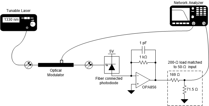
The amplifier was tested in a transimpedance configuration by using a photodiode with an optical fiber input connection. A tunable laser connected through an optical modulator was used to create the modulated optical excitation to the photodiode. Figure 9-2 shows the test setup configuration for the frequency response measurement. The network analyzer's swept frequency output drives the optical modulators electrical input which in turn drives the photodiode. The OPA856 output drives the network analyzer's input.
 Figure 9-2 OPA856 Transimpedance Frequency Response Test Setup
Figure 9-4 shows the frequency response measurements for a small signal and large signal (~1 Vpp) output. The plot contains noticeable noise and variations because the test environment did not have complete capability to accurately manage the thermal drift, perform optical connection integrity analysis, and calibrate the optical path. A more stringently controlled optical environment could achieve more stable results, but was beyond the scope of these measurements. The results in Figure 9-4 correlate well with predicted results of approximately 200 MHz of bandwidth. It is expected that the results would not perfectly match calculated values because it is challenging to perfectly account for all parasitic capacitances that affect the input and feedback capacitance in the transimpedance calculations.
Many transimpedance applications can have unpredicted, large input currents that can cause the amplifier's output to saturate. It is often important to understand how the amplifier will behave when its output is saturated at various levels of overdrive. A typical linear amplifier like the OPA856 can be expected to have an output saturation recovery time that increases as the amount of output overdrive increases. When using a pulse based input signal, the output saturation recovery time effectively extends the duration of the pulse. Figure 9-3 shows the test setup configuration to measure a pulsed optical input to the OPA856. The optical modulator used in the test setup had limited output amplitude capability to create a saturated signal. In order to prevent the modulator from saturating, the OPA856 output was saturated by adjusting VOFFSET close to the the amplifier's output swing limit on the negative rail.
 Figure 9-3 OPA856 Transimpedance Pulse Saturation Extention Test Setup
Figure 9-5 shows the resulting shifted output pulses labelled by the magnitude of voltage they are overdriving the amplifiers output saturation voltage level (VOV). These values only serve as approximations of the overdrive level of the signal because of expected variances from the optical interface setup. Figure 9-6 shows a magnified view of the rising edge of the measured pulse responses in order to better detail the pulse extension created by the signal overdrive. These plots have been scaled and normalized to be easier to read and compare. As expected, Figure 9-6 shows that the pulse duration is extended as the overdrive level increases. The data only captured an overdrive voltage maximum of 640 mV, but it can be expected that larger voltages would extend the pulse further.