JAJSJX2 October   2020 OPA856

PRODUCTION DATA  

  1. 特長
  2. アプリケーション
  3. 概要
  4. Revision History
  5. Device Comparison Table
  6. Pin Configuration and Functions
    1.     Pin Functions
  7. Specifications
    1. 7.1 Absolute Maximum Ratings
    2. 7.2 ESD Ratings
    3. 7.3 Recommended Operating Conditions
    4. 7.4 Thermal Information
    5. 7.5 Electrical Characteristics
    6. 7.6 Typical Characteristics
    7. 7.7 Typical Characteristics (continued)
  8. Detailed Description
    1. 8.1 Overview
    2. 8.2 Functional Block Diagram
    3. 8.3 Feature Description
      1. 8.3.1 Input and ESD Protection
      2. 8.3.2 Feedback Pin
      3. 8.3.3 Wide Gain-Bandwidth Product
      4. 8.3.4 Slew Rate and Output Stage
    4. 8.4 Device Functional Modes
      1. 8.4.1 Split-Supply and Single-Supply Operation
      2. 8.4.2 Power-Down Mode
  9. Application and Implementation
    1. 9.1 Application Information
    2. 9.2 Typical Application
      1. 9.2.1 Design Requirements
      2. 9.2.2 Detailed Design Procedure
      3. 9.2.3 Application Curves
  10. 10Power Supply Recommendations
  11. 11Layout
    1. 11.1 Layout Guidelines
    2. 11.2 Layout Example
  12. 12Device and Documentation Support
    1. 12.1 Device Support
      1. 12.1.1 Development Support
    2. 12.2 Documentation Support
      1. 12.2.1 Related Documentation
    3. 12.3 Receiving Notification of Documentation Updates
    4. 12.4 サポート・リソース
    5. 12.5 Trademarks
    6. 12.6 Electrostatic Discharge Caution
    7. 12.7 Glossary
  13. 13Mechanical, Packaging, and Orderable Information

パッケージ・オプション

メカニカル・データ(パッケージ|ピン)
サーマルパッド・メカニカル・データ
発注情報

Power-Down Mode

The OPA856 features a power-down mode to reduce the quiescent current to conserve power. Figure 7-19 and Figure 7-20 show the transient response of the OPA856 as the PD pin toggles between the disabled and enabled states.

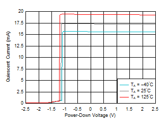
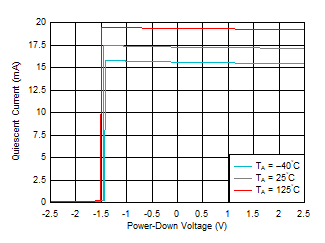
The PD disable and enable threshold voltages are with reference to the negative supply. If the amplifier is configured with the positive supply at 3.3 V and the negative supply at ground, then the disable and enable threshold voltages are 0.65 V and 1.8 V, respectively. If the amplifier is configured with ±1.65 V supplies, then the threshold voltages are at –1 V and 0.15 V. If the amplifier is configured with ±2.5 V supplies, then the threshold voltages are at –1.85 V and –0.7 V.

Figure 8-8 shows the switching behavior of a typical amplifier as the PD pin is swept down from the enabled state to the disabled state. Similarly, Figure 8-9 shows the switching behavior of a typical amplifier as the PD pin is swept up from the disabled state to the enabled state. The small difference in the switching thresholds between the down sweep and the up sweep is caused by the hysteresis designed into the amplifier to increase immunity to noise on the PD pin.
GUID-20200917-CA0I-B2Q1-FMMG-8R3Q5Z0Q1WJ6-low.gifFigure 8-8 Switching Threshold
(PD Pin Swept from High to Low)
GUID-20200917-CA0I-TBNZ-GN5H-CSJLQGQ99NN9-low.gifFigure 8-9 Switching Threshold
(PD Pin Swept from Low to High)
Connecting the PD pin low disables the amplifier and places the output in a high-impedance state. When the amplifier is configured as a noninverting amplifier, the feedback (RF) and gain (RG) resistor network form a parallel load to the output of the amplifier. To protect the input stage of the amplifier, the OPA856 uses internal, back-to-back protection diodes between the inverting and noninverting input pins as Figure 8-3 shows. In the power-down state, if the differential voltage between the input pins of the amplifier exceeds a diode voltage drop, an additional low-impedance path is created between the noninverting input pin and the output pin.