JAJSJX2 October   2020 OPA856

PRODUCTION DATA  

  1. 特長
  2. アプリケーション
  3. 概要
  4. Revision History
  5. Device Comparison Table
  6. Pin Configuration and Functions
    1.     Pin Functions
  7. Specifications
    1. 7.1 Absolute Maximum Ratings
    2. 7.2 ESD Ratings
    3. 7.3 Recommended Operating Conditions
    4. 7.4 Thermal Information
    5. 7.5 Electrical Characteristics
    6. 7.6 Typical Characteristics
    7. 7.7 Typical Characteristics (continued)
  8. Detailed Description
    1. 8.1 Overview
    2. 8.2 Functional Block Diagram
    3. 8.3 Feature Description
      1. 8.3.1 Input and ESD Protection
      2. 8.3.2 Feedback Pin
      3. 8.3.3 Wide Gain-Bandwidth Product
      4. 8.3.4 Slew Rate and Output Stage
    4. 8.4 Device Functional Modes
      1. 8.4.1 Split-Supply and Single-Supply Operation
      2. 8.4.2 Power-Down Mode
  9. Application and Implementation
    1. 9.1 Application Information
    2. 9.2 Typical Application
      1. 9.2.1 Design Requirements
      2. 9.2.2 Detailed Design Procedure
      3. 9.2.3 Application Curves
  10. 10Power Supply Recommendations
  11. 11Layout
    1. 11.1 Layout Guidelines
    2. 11.2 Layout Example
  12. 12Device and Documentation Support
    1. 12.1 Device Support
      1. 12.1.1 Development Support
    2. 12.2 Documentation Support
      1. 12.2.1 Related Documentation
    3. 12.3 Receiving Notification of Documentation Updates
    4. 12.4 サポート・リソース
    5. 12.5 Trademarks
    6. 12.6 Electrostatic Discharge Caution
    7. 12.7 Glossary
  13. 13Mechanical, Packaging, and Orderable Information

パッケージ・オプション

メカニカル・データ(パッケージ|ピン)
サーマルパッド・メカニカル・データ
発注情報

Application Curves

Note: Figure 9-6 output voltages are scaled for visual comparison purposes and are not the actual measured values. See Figure 9-5 for actual measured values.
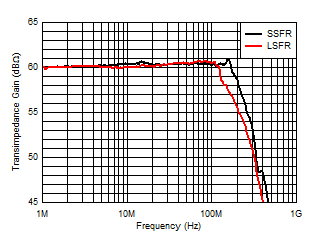
GUID-20200921-CA0I-FS2B-HJDD-7NTHLVT64DLT-low.gifFigure 9-4 Transimpedance Frequency Response
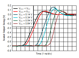
GUID-20200921-CA0I-NDXX-3BVH-HPD21KBXBCSX-low.gifFigure 9-6 Transimpedance Pulse Response Magnified and Scaled
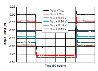
GUID-20200921-CA0I-H11R-LPW9-ZWWVJSWNDGW5-low.gifFigure 9-5 Transimpedance Pulse Response