JAJSJX2 October   2020 OPA856

PRODUCTION DATA  

  1. 特長
  2. アプリケーション
  3. 概要
  4. Revision History
  5. Device Comparison Table
  6. Pin Configuration and Functions
    1.     Pin Functions
  7. Specifications
    1. 7.1 Absolute Maximum Ratings
    2. 7.2 ESD Ratings
    3. 7.3 Recommended Operating Conditions
    4. 7.4 Thermal Information
    5. 7.5 Electrical Characteristics
    6. 7.6 Typical Characteristics
    7. 7.7 Typical Characteristics (continued)
  8. Detailed Description
    1. 8.1 Overview
    2. 8.2 Functional Block Diagram
    3. 8.3 Feature Description
      1. 8.3.1 Input and ESD Protection
      2. 8.3.2 Feedback Pin
      3. 8.3.3 Wide Gain-Bandwidth Product
      4. 8.3.4 Slew Rate and Output Stage
    4. 8.4 Device Functional Modes
      1. 8.4.1 Split-Supply and Single-Supply Operation
      2. 8.4.2 Power-Down Mode
  9. Application and Implementation
    1. 9.1 Application Information
    2. 9.2 Typical Application
      1. 9.2.1 Design Requirements
      2. 9.2.2 Detailed Design Procedure
      3. 9.2.3 Application Curves
  10. 10Power Supply Recommendations
  11. 11Layout
    1. 11.1 Layout Guidelines
    2. 11.2 Layout Example
  12. 12Device and Documentation Support
    1. 12.1 Device Support
      1. 12.1.1 Development Support
    2. 12.2 Documentation Support
      1. 12.2.1 Related Documentation
    3. 12.3 Receiving Notification of Documentation Updates
    4. 12.4 サポート・リソース
    5. 12.5 Trademarks
    6. 12.6 Electrostatic Discharge Caution
    7. 12.7 Glossary
  13. 13Mechanical, Packaging, and Orderable Information

パッケージ・オプション

メカニカル・データ(パッケージ|ピン)
サーマルパッド・メカニカル・データ
発注情報

Typical Application

The high GBWP of the OPA856 makes the device an excellent choice as a transimpedance amplifier while the unity gain stability allows for use of feedback clamping or other unity gain circuitry that would not work for a decompensated amplifier. Figure 9-1 shows the OPA856 configured as a transimpedance amplifier with an option feedback clamping diode connection.
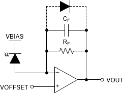
GUID-20200921-CA0I-WDHF-KDHJ-7C28FWLHQGK1-low.gif Figure 9-1 OPA856 Transimpedance Amplifier with Optional Diode Clamping