JAJSJX2 October 2020 OPA856
PRODUCTION DATA
- 1 特長
- 2 アプリケーション
- 3 概要
- 4 Revision History
- 5 Device Comparison Table
- 6 Pin Configuration and Functions
- 7 Specifications
- 8 Detailed Description
- 9 Application and Implementation
- 10Power Supply Recommendations
- 11Layout
- 12Device and Documentation Support
- 13Mechanical, Packaging, and Orderable Information
パッケージ・オプション
メカニカル・データ(パッケージ|ピン)
- DSG|8
サーマルパッド・メカニカル・データ
- DSG|8
発注情報
8.3.2 Feedback Pin
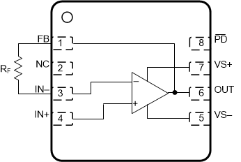
The OPA856 pin layout is optimized to minimize parasitic inductance and capacitance, which is a critical care about in high-speed analog design. The FB pin (pin 1) is internally connected to the output of the amplifier. The FB pin is separated from the inverting input of the amplifier (pin 3) by a no connect (NC) pin (pin 2). The NC pin must be left floating. There are two advantages to this pin layout:
- A feedback resistor (RF) can connect between the FB and IN– pin on the same side of the package (see Figure 8-4) rather than going around the package.
- The isolation created by the NC pin minimizes the capacitive coupling between the FB and IN– pins by increasing the physical separation between the pins.
 Figure 8-4 RF Connection Between FB and IN– Pins