JAJSKI5 February 2021 OPA859-Q1
PRODUCTION DATA
- 1 特長
- 2 アプリケーション
- 3 概要
- 4 Revision History
- 5 Pin Configuration and Functions
- 6 Specifications
- 7 Parameter Measurement Information
- 8 Detailed Description
- 9 Application and Implementation
- 10Power Supply Recommendations
- 11Layout
- 12Device and Documentation Support
- 13Mechanical, Packaging, and Orderable Information
9.2.2 Detailed Design Procedure
The OPA859-Q1 meets the growing demand for wideband, low-noise photodiode amplifiers. The closed-loop bandwidth of a transimpedance amplifier is a function of the following:
- The total input capacitance (CIN). This total includes the photodiode capacitance, the input capacitance of the amplifier (common-mode and differential capacitance) and any stray capacitance from the PCB.
- The op amp gain bandwidth product (GBWP).
- The transimpedance gain (RF).
Figure 9-1 shows the OPA859-Q1 configured as a TIA, with the avalanche photodiode (APD) reverse biased so that the APD cathode is tied to a large positive bias voltage. In this configuration, the APD sources current into the op amp feedback loop so that the output swings in a negative direction relative to the input common-mode voltage. To maximize the output swing in the negative direction, the OPA859-Q1 common-mode voltage is set close to the positive limit; only 1.5 V from the positive supply rail. The feedback resistance (RF) and the input capacitance (CIN) form a zero in the noise gain that results in instability if left unchecked. To counteract the effect of the zero, a pole is inserted into the noise gain transfer function by adding the feedback capacitor (CF).
The Transimpedance Considerations for High-Speed Amplifiers Application Report discusses theories and equations that show how to compensate a transimpedance amplifier for a particular transimpedance gain and input capacitance. The bandwidth and compensation equations from the application report are available in an Excel® calculator. What You Need To Know About Transimpedance Amplifiers – Part 1 provides a link to the calculator.
The equations and calculators in the referenced application report and blog posts are used to model the bandwidth (f–3dB) and noise (IRN) performance of the OPA859-Q1 configured as a TIA. The resultant performance is shown in Figure 9-2 and Figure 9-3. The left-side Y-axis shows the closed-loop bandwidth performance, whereas the right side of the graph shows the integrated input-referred noise. The noise bandwidth to calculate IRN for a fixed RF and CPD is set equal to the f–3dB frequency. Figure 9-2 shows the amplifier performance as a function of photodiode capacitance (CPD) for RF = 10 kΩ and 20 kΩ. Increasing CPD decreases the closed-loop bandwidth. To maximize bandwidth, make sure to reduce any stray parasitic capacitance from the PCB. The OPA859-Q1 is designed with 0.8 pF of total input capacitance to minimize the effect of stray capacitance on system performance. Figure 9-3 shows the amplifier performance as a function of RF for CPD = 1 pF and 2 pF. Increasing RF results in lower bandwidth. To maximize the signal-to-noise ratio (SNR) in an optical front-end system, maximize the gain in the TIA stage. Increasing RF by a factor of X increases the signal level by X, but only increases the resistor noise contribution by √X, thereby improving SNR.
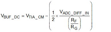
The OPA859-Q1 configured as a unity-gain buffer drives a dc offset voltage of 2.95 V into the lower half of the THS4520. To maximize the dynamic range of the ADC, the two OPA859 amplifiers drive a differential common-mode of 3.5 V and 2.95 V into the THS4520. The dc offset voltage of the buffer amplifier can be derived using Equation 1.
where
- VTIA_CM is the common-mode voltage of the TIA (3.5 V)
- VADC_DIFF_IN is the differential input voltage range of the ADC (1.1 VPP)
- RF and RG are the feedback resistance (499 Ω) and gain resistance (499 Ω) of the THS4520 differential amplifier
The low-pass filter between the THS4520 and the ADC54J64 minimizes high-frequency noise and maximizes SNR. The ADC54J64 has an internal buffer that isolates the output of the THS4520 from the ADC sampling-capacitor input, so a traditional charge bucket filter is not required.