JAJSVR9K
December 2005 – December 2024
PCA9557
PRODUCTION DATA
1
1
特長
2
アプリケーション
3
概要
4
Pin Configuration and Functions
5
Specifications
5.1
Absolute Maximum Ratings
5.2
ESD Ratings
5.3
Recommended Operating Conditions
5.4
Thermal Information
5.5
Electrical Characteristics
5.6
I2C Interface Timing Requirements
5.7
Reset Timing Requirements
5.8
Switching Characteristics
5.9
Typical Characteristics
6
Parameter Measurement Information
7
Detailed Description
7.1
Functional Block Diagram
7.2
Feature Description
7.2.1
RESET
7.2.1.1
RESET Errata
7.2.1.1.1
System Impact
7.2.1.1.2
System Workaround
7.2.2
Power-On Reset
7.3
Programming
7.3.1
I2C Interface
7.4
Register Maps
7.4.1
Device Address
7.4.2
Control Register And Command Byte
7.4.3
Register Descriptions
7.4.3.1
Bus Transactions
7.4.3.1.1
Writes
7.4.3.1.2
Reads
8
Application and Implementation
8.1
Application Information
8.2
Typical Application
8.2.1
Detailed Design Procedure
8.2.1.1
Minimizing ICC when I/O is Used to Control LED
8.3
Power Supply Recommendations
8.3.1
Power-On Reset Errata
8.3.1.1
System Impact
9
Device and Documentation Support
9.1
Documentation Support
9.1.1
Related Documentation
9.2
Receiving Notification of Documentation Updates
9.3
サポート・リソース
9.4
Trademarks
9.5
静電気放電に関する注意事項
9.6
用語集
10
Revision History
11
Mechanical, Packaging, and Orderable Information
パッケージ・オプション
メカニカル・データ(パッケージ|ピン)
DGV|16
MPDS006C
PW|16
MPDS361A
DB|16
MPDS507A
RGY|16
MPQF115G
D|16
MPDS178G
RGV|16
MPQF121F
サーマルパッド・メカニカル・データ
RGY|16
QFND040P
RGV|16
QFND107G
発注情報
jajsvr9k_oa
jajsvr9k_pm
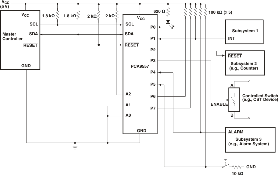
8.2
Typical Application
A.
Device address is configured as 0011100 for this example.
B.
P1, P4, and P5 are configured as inputs.
C.
P0, P2, and P3 are configured as outputs.
D.
P6 and P7 are not used and must be configured as outputs.
Figure 8-1
Typical Application