SLES248A May 2009 – March 2015 PCM1795
PRODUCTION DATA.
- 1 Features
- 2 Applications
- 3 Description
- 4 Revision History
- 5 Pin Configuration and Functions
- 6 Specifications
-
7 Detailed Description
- 7.1 Overview
- 7.2 Functional Block Diagram
- 7.3 Feature Description
- 7.4 Device Functional Modes
- 7.5 Programming
- 7.6
Register Maps
- 7.6.1
Mode Control Registers
- 7.6.1.1 User-Programmable Mode Controls
- 7.6.1.2 Register Map
- 7.6.1.3
Register Definitions
- 7.6.1.3.1 R/W: Read/Write Mode Select
- 7.6.1.3.2 ATx[7:0]: Digital Attenuation Level Setting
- 7.6.1.3.3 R/W: Read/Write Mode Select
- 7.6.1.3.4 ATLD: Attenuation Load Control
- 7.6.1.3.5 FMT[2:0]: Audio Interface Data Format
- 7.6.1.3.6 DMF[1:0]: Sampling Frequency Selection for the De-Emphasis Function
- 7.6.1.3.7 DME: Digital De-Emphasis Control
- 7.6.1.3.8 MUTE: Soft Mute Control
- 7.6.1.3.9 R/W: Read/Write Mode Select
- 7.6.1.3.10 REV: Output Phase Reversal
- 7.6.1.3.11 ATS[1:0]: Attenuation Rate Select
- 7.6.1.3.12 OPE: DAC Operation Control
- 7.6.1.3.13 DFMS: Stereo DF Bypass Mode Select
- 7.6.1.3.14 FLT: Digital Filter Roll-Off Control
- 7.6.1.3.15 INZD: Infinite Zero Detect Mute Control
- 7.6.1.3.16 R/W: Read/Write Mode Select
- 7.6.1.3.17 SRST: System Reset Control
- 7.6.1.3.18 DSD: DSD Interface Mode Control
- 7.6.1.3.19 DFTH: Digital Filter Bypass (or Through Mode) Control
- 7.6.1.3.20 MONO: Monaural Mode Selection
- 7.6.1.3.21 CHSL: Channel Selection for Monaural Mode
- 7.6.1.3.22 OS[1:0]: ΔΣ Oversampling Rate Selection
- 7.6.1.3.23 R/W: Read/Write Mode Select
- 7.6.1.3.24 DZ[1:0]: DSD Zero Output Enable
- 7.6.1.3.25 PCMZ: PCM Zero Output Enable
- 7.6.1.3.26 R: Read Mode Select
- 7.6.1.3.27 ZFGx: Zero-Detection Flag
- 7.6.1.3.28 Read Mode Select
- 7.6.1.3.29 ID[4:0]: Device ID
- 7.6.1
Mode Control Registers
-
8 Application and Implementation
- 8.1 Application Information
- 8.2
Typical Applications
- 8.2.1 Typical Connection Diagram in PCM Mode
- 8.2.2
Application for External Digital Filter Interface
- 8.2.2.1 Design Requirements
- 8.2.2.2 Detailed Design Procedure
- 8.2.2.3 Application Curves
- 8.2.3 Application for DSD Format (DSD Mode) Interface
- 8.2.4
TDMCA Interface Format
- 8.2.4.1 Design Requirements
- 8.2.4.2
Detailed Design Procedure
- 8.2.4.2.1 TDMCA Mode Determination
- 8.2.4.2.2 TDMCA Terminals
- 8.2.4.2.3 Device ID Determination
- 8.2.4.2.4 TDMCA Frame
- 8.2.4.2.5
Command Field
- 8.2.4.2.5.1 Bit 31: Device ID Enable Flag
- 8.2.4.2.5.2 Bit 30: Extended Command Enable Flag
- 8.2.4.2.5.3 Bit 29: Daisy-Chain Selection Flag
- 8.2.4.2.5.4 Bits[28:24]: Device ID
- 8.2.4.2.5.5 Bit 23: Command Read/Write flag
- 8.2.4.2.5.6 Bits[22:16]: Register ID
- 8.2.4.2.5.7 Bits[15:8]: Command data
- 8.2.4.2.5.8 Bits[7:0]: Not used
- 8.2.4.2.6 Extended Command Field
- 8.2.4.2.7 Audio Fields
- 8.2.4.2.8 TDMCA Register Requirements
- 8.2.4.2.9 Register Write/Read Operation
- 8.2.4.2.10 TDMCA Mode Operation
- 9 Power Supply Recommendations
- 10Layout
- 11Device and Documentation Support
- 12Mechanical, Packaging, and Orderable Information
1 Features
- 32-Bit Resolution
- Analog Performance:
- Dynamic Range: 123 dB
- THD+N: 0.0005%
- Differential Current Output: 3.9 mAPP
- 8× Oversampling Digital Filter:
- Stop-Band Attenuation: –98 dB
- Passband Ripple: ±0.0002 dB
- Sampling Frequency: 10 kHz to 200 kHz
- System Clock: 128, 192, 256, 384, 512,
or 768 fS With Autodetect - Accepts 16-, 24-, and 32-Bit Audio Data
- PCM Data Formats: Standard, I2S, and Left-Justified
- DSD Format Interface Available
- Interface Available for Optional External Digital Filter or DSP
- TDMCA or Serial Port (SPI™/I2C)
- User-Programmable Mode Controls:
- Digital Attenuation:
0 dB to –120 dB, 0.5-dB/Step - Digital De-Emphasis
- Digital Filter Roll-Off: Sharp or Slow
- Soft Mute
- Zero Flag for Each Output
- Digital Attenuation:
- Compatible With PCM1792A and PCM1796
(Pins and Mode Controls) - Dual Supply Operation:
- 5-V Analog, 3.3-V Digital
- 5-V Tolerant Digital Inputs
- Small SSOP-28 Package
2 Applications
- A/V Receivers
- SACD Players
- DVD Players
- HDTV Receivers
- Car Audio Systems
- Digital Multitrack Recorders
- Other Applications Requiring 32-Bit Audio
3 Description
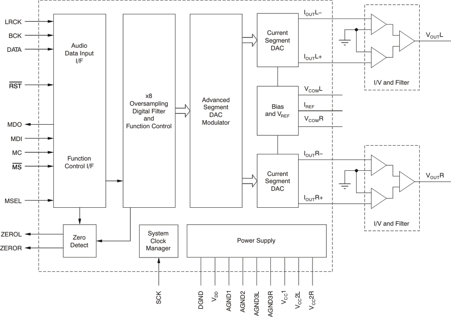
The PCM1795 device is a monolithic CMOS integrated circuit that includes stereo digital-to-analog converters (DACs) and support circuitry in a small SSOP-28 package. The data converters use TI’s advanced segment DAC architecture to achieve excellent dynamic performance and improved tolerance to clock jitter. The PCM1795 provides balanced current outputs, letting the user optimize analog performance externally. The PCM1795 accepts pulse code modulation (PCM) and direct stream digital (DSD) audio data formats, thus providing an easy interface to audio digital signal processors (DSPs) and decoder chips. The PCM1795 device also interfaces with external digital filter devices such as the DF1704, DF1706, and the PMD200 from Pacific Microsonics™. Sampling rates up to 200 kHz are supported. A full set of user-programmable functions is accessible through an SPI or I2C serial control port that supports register write and readback functions. The PCM1795 device also supports the time-division-multiplexed (TDM) command and audio (TDMCA) data format.
Device Information(1)
| PART NUMBER | PACKAGE | BODY SIZE (NOM) |
|---|---|---|
| PCM1795 | SSOP (28) | 10.20 mm × 5.30 mm |
- For all available packages, see the orderable addendum at the end of the data sheet.
Block Diagram

4 Revision History
Changes from * Revision (May 2009) to A Revision
- Added Pin Configuration and Functions section, ESD Rating table, Recommended Operating Conditions table, Feature Description section, Device Functional Modes, Application and Implementation section, Power Supply Recommendations section, Layout section, Device and Documentation Support section, and Mechanical, Packaging, and Orderable Information section Go