SLES230A September 2008 – August 2015 PCM2912A
PRODUCTION DATA.
- 1 Features
- 2 Applications
- 3 Description
- 4 Revision History
- 5 Device Comparison Table
- 6 Pin Configuration and Functions
-
7 Specifications
- 7.1 Absolute Maximum Ratings
- 7.2 ESD Ratings
- 7.3 Recommended Operating Conditions
- 7.4 Thermal Information
- 7.5 Electrical Characteristics
- 7.6
Typical Characteristics
- 7.6.1 ADC Digital Decimation Filter Frequency Response
- 7.6.2 ADC Digital High-Pass Filter Frequency Response
- 7.6.3 ADC Analog Antialiasing Filter Frequency Response
- 7.6.4 DAC Digital Interpolation Filter Frequency Response
- 7.6.5 DAC Analog FIR Filter Frequency Response
- 7.6.6 DAC Analog Low-Pass Filter Frequency Response
- 7.6.7 ADC
- 7.6.8 DAC
- 7.6.9 Supply Current
- 8 Parameter Measurement Information
-
9 Detailed Description
- 9.1 Overview
- 9.2 Functional Block Diagram
- 9.3 Feature Description
- 9.4 Device Functional Modes
- 9.5 Programming
- 10Application and Implementation
- 11Power Supply Recommendations
- 12Layout
- 13Device and Documentation Support
- 14Mechanical, Packaging, and Orderable Information
12 Layout
12.1 Layout Guidelines
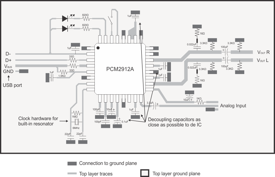
The decoupling capacitors must be as close as possible to the PCM2912A pins. TI recommends following the output filter for the headphone amplifier used in the PCM2912A EVM. The analog input needs a series capacitor to eliminate any possible offset level. The PCM2912A is a low-power device, thus there is no need for a special heat sink PCB design.
12.2 Layout Example
