SLES230A September 2008 – August 2015 PCM2912A
PRODUCTION DATA.
- 1 Features
- 2 Applications
- 3 Description
- 4 Revision History
- 5 Device Comparison Table
- 6 Pin Configuration and Functions
-
7 Specifications
- 7.1 Absolute Maximum Ratings
- 7.2 ESD Ratings
- 7.3 Recommended Operating Conditions
- 7.4 Thermal Information
- 7.5 Electrical Characteristics
- 7.6
Typical Characteristics
- 7.6.1 ADC Digital Decimation Filter Frequency Response
- 7.6.2 ADC Digital High-Pass Filter Frequency Response
- 7.6.3 ADC Analog Antialiasing Filter Frequency Response
- 7.6.4 DAC Digital Interpolation Filter Frequency Response
- 7.6.5 DAC Analog FIR Filter Frequency Response
- 7.6.6 DAC Analog Low-Pass Filter Frequency Response
- 7.6.7 ADC
- 7.6.8 DAC
- 7.6.9 Supply Current
- 8 Parameter Measurement Information
-
9 Detailed Description
- 9.1 Overview
- 9.2 Functional Block Diagram
- 9.3 Feature Description
- 9.4 Device Functional Modes
- 9.5 Programming
- 10Application and Implementation
- 11Power Supply Recommendations
- 12Layout
- 13Device and Documentation Support
- 14Mechanical, Packaging, and Orderable Information
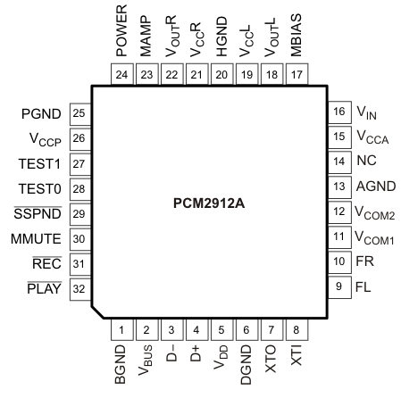
6 Pin Configuration and Functions
PJT Package
32-Pin TQFP
Top View

Pin Functions
| PIN | I/O | DESCRIPTION | |
|---|---|---|---|
| NAME | NO. | ||
| AGND | 13 | — | Analog ground |
| BGND | 1 | — | Reference for internal regulator |
| D– | 3 | I/O | USB differential input/output minus(1) |
| D+ | 4 | I/O | USB differential input/output plus(1) |
| DGND | 6 | Digital ground | |
| FL | 9 | — | External filter pin of L-channel (optional) |
| FR | 10 | — | External filter pin of R-channel (optional) |
| HGND | 20 | — | Analog ground for headphone amplifier |
| MAMP | 23 | I | Microphone preamplifier gain control (LOW: Preamplifier off, HIGH: Preamplifier on = +20 dB)(2) |
| MBIAS | 17 | O | Microphone bias output (0.75 VCCA) |
| MMUTE | 30 | I | Microphone mute control, active HIGH (LOW: Mute off, HIGH: Mute on)(3) |
| NC | 14 | — | Not connected |
| PGND | 25 | — | Analog ground for microphone bias, microphone amplifier, and PGA |
| PLAY | 32 | O | Status output for playback (LOW: Playback, FLASH: Mute on playback, HIGH: Stop)(5) |
| POWER | 24 | I | Power consumption declaration select pin (LOW: 100 mA, HIGH: 500 mA) (2) |
| REC | 31 | O | Status output for record (LOW: Record, FLASH: Mute on recode, HIGH: Stop)(5) |
| SSPND | 29 | O | Suspend flag (LOW: Suspend, HIGH: Operational state) |
| TEST0 | 28 | I | Test pin. Must be set to LOW(2) |
| TEST1 | 27 | I | Test pin. Must be set to HIGH(2) |
| VBUS | 2 | — | Connect to USB power (VBUS) |
| VCCA | 15 | — | Analog power supply |
| VCCL | 19 | — | Analog power supply for headphone amplifier of L-channel(4) |
| VCCP | 26 | — | Analog power supply for PLL(4) |
| VCCR | 21 | — | Analog power supply for headphone amplifier of R-channel(4) |
| VCOM1 | 11 | — | Common voltage for ADC, DAC, and analog front-end (VCCA/2). Decoupling capacitor must be connected to AGND. |
| VCOM2 | 12 | — | Common voltage for headphone (VCCA/2). Decoupling capacitor must be connected to AGND. |
| VDD | 5 | — | Digital power supply(4) |
| VIN | 16 | I | ADC microphone input |
| VOUTL | 18 | O | Headphone output for L-channel |
| VOUTR | 22 | O | Headphone output for R-channel |
| XTI | 8 | I | Crystal oscillator input(2) |
| XTO | 7 | O | Crystal oscillator output |
(1) LV-TTL level
(2) 3.3-V CMOS level input.
(3) 3.3-V CMOS level input with internal pulldown resistor.
(4) Connect decoupling capacitor to corresponding ground.
(5) 5-V tolerant, open-drain.