JAJSNF3A April   2022  – August 2022 PCM6120-Q1

PRODUCTION DATA  

  1. 特長
  2. アプリケーション
  3. 概要
  4. Revision History
  5. Device Comparison Table
  6. Pin Configuration and Functions
  7. Specifications
    1. 7.1  Absolute Maximum Ratings
    2. 7.2  ESD Ratings
    3. 7.3  Recommended Operating Conditions
    4.     Thermal Information
    5. 7.4  Electrical Characteristics
    6. 7.5  Timing Requirements: I2C Interface
    7. 7.6  Switching Characteristics: I2C Interface
    8. 7.7  Timing Requirements: TDM, I2S or LJ Interface
    9. 7.8  Switching Characteristics: TDM, I2S or LJ Interface
    10.     Timing Requirements: PDM Digital Microphone Interface
    11. 7.9  Switching Characteristics: PDM Digial Microphone Interface
    12. 7.10 Timing Diagrams
    13. 7.11 Typical Characteristics
  8. Detailed Description
    1. 8.1 Overview
    2. 8.2 Functional Block Diagram
    3. 8.3 Feature Description
      1. 8.3.1  Serial Interfaces
        1. 8.3.1.1 Control Serial Interfaces
        2. 8.3.1.2 Audio Serial Interfaces
          1. 8.3.1.2.1 Time Division Multiplexed Audio (TDM) Interface
          2. 8.3.1.2.2 Inter IC Sound (I2S) Interface
          3. 8.3.1.2.3 Left-Justified (LJ) Interface
        3. 8.3.1.3 Using Multiple Devices With Shared Buses
      2. 8.3.2  Phase-Locked Loop (PLL) and Clock Generation
      3. 8.3.3  Input Channel Configurations
      4. 8.3.4  Reference Voltage
      5. 8.3.5  Programmable Microphone Bias
      6. 8.3.6  Signal-Chain Processing
        1. 8.3.6.1 Programmable Channel Gain and Digital Volume Control
        2. 8.3.6.2 Programmable Channel Gain Calibration
        3. 8.3.6.3 Programmable Channel Phase Calibration
        4. 8.3.6.4 Programmable Digital High-Pass Filter
        5. 8.3.6.5 Programmable Digital Biquad Filters
        6. 8.3.6.6 Programmable Channel Summer and Digital Mixer
        7. 8.3.6.7 Configurable Digital Decimation Filters
          1. 8.3.6.7.1 Linear Phase Filters
            1. 8.3.6.7.1.1 Sampling Rate: 7.35 kHz to 8 kHz
            2. 8.3.6.7.1.2 Sampling Rate: 14.7 kHz to 16 kHz
            3. 8.3.6.7.1.3 Sampling Rate: 22.05 kHz to 24 kHz
            4. 8.3.6.7.1.4 Sampling Rate: 29.4 kHz to 32 kHz
            5. 8.3.6.7.1.5 Sampling Rate: 44.1 kHz to 48 kHz
            6. 8.3.6.7.1.6 Sampling Rate: 88.2 kHz to 96 kHz
            7. 8.3.6.7.1.7 Sampling Rate: 176.4 kHz to 192 kHz
            8. 8.3.6.7.1.8 Sampling Rate: 352.8 kHz to 384 kHz
            9. 8.3.6.7.1.9 Sampling Rate: 705.6 kHz to 768 kHz
          2. 8.3.6.7.2 Low-Latency Filters
            1. 8.3.6.7.2.1 Sampling Rate: 14.7 kHz to 16 kHz
            2. 8.3.6.7.2.2 Sampling Rate: 22.05 kHz to 24 kHz
            3. 8.3.6.7.2.3 Sampling Rate: 29.4 kHz to 32 kHz
            4. 8.3.6.7.2.4 Sampling Rate: 44.1 kHz to 48 kHz
            5. 8.3.6.7.2.5 Sampling Rate: 88.2 kHz to 96 kHz
            6. 8.3.6.7.2.6 Sampling Rate: 176.4 kHz to 192 kHz
          3. 8.3.6.7.3 Ultra-Low Latency Filters
            1. 8.3.6.7.3.1 Sampling Rate: 14.7 kHz to 16 kHz
            2. 8.3.6.7.3.2 Sampling Rate: 22.05 kHz to 24 kHz
            3. 8.3.6.7.3.3 Sampling Rate: 29.4 kHz to 32 kHz
            4. 8.3.6.7.3.4 Sampling Rate: 44.1 kHz to 48 kHz
            5. 8.3.6.7.3.5 Sampling Rate: 88.2 kHz to 96 kHz
            6. 8.3.6.7.3.6 Sampling Rate: 176.4 kHz to 192 kHz
            7. 8.3.6.7.3.7 Sampling Rate: 352.8 kHz to 384 kHz
      7. 8.3.7  Dynamic Range Enhancer (DRE)
      8. 8.3.8  Dynamic Range Compressor (DRC)
      9. 8.3.9  Automatic Gain Controller (AGC)
      10. 8.3.10 Voice Activity Detection (VAD)
      11. 8.3.11 Digital PDM Microphone Record Channel
      12. 8.3.12 Interrupts, Status, and Digital I/O Pin Multiplexing
    4. 8.4 Device Functional Modes
      1. 8.4.1 Sleep Mode or Software Shutdown
      2. 8.4.2 Active Mode
      3. 8.4.3 Software Reset
    5. 8.5 Programming
      1. 8.5.1 Control Serial Interfaces
        1. 8.5.1.1 I2C Control Interface
          1. 8.5.1.1.1 General I2C Operation
            1. 8.5.1.1.1.1 I2C Single-Byte and Multiple-Byte Transfers
              1. 8.5.1.1.1.1.1 I2C Single-Byte Write
              2. 8.5.1.1.1.1.2 I2C Multiple-Byte Write
              3. 8.5.1.1.1.1.3 I2C Single-Byte Read
              4. 8.5.1.1.1.1.4 I2C Multiple-Byte Read
    6. 8.6 Register Maps
      1. 8.6.1 Device Configuration Registers
        1. 8.6.1.1 PCM6120-Q1 Access Codes
      2. 8.6.2 Page 0 Registers
      3. 8.6.3 Page 1 Registers
      4. 8.6.4 Programmable Coefficient Registers
        1. 8.6.4.1 Programmable Coefficient Registers: Page 2
        2. 8.6.4.2 Programmable Coefficient Registers: Page 3
        3. 8.6.4.3 Programmable Coefficient Registers: Page 4
  9. Application and Implementation
    1. 9.1 Application Information
    2. 9.2 Typical Applications
      1. 9.2.1 Two-Channel Analog Microphone Recording
        1. 9.2.1.1 Design Requirements
        2. 9.2.1.2 Detailed Design Procedure
          1. 9.2.1.2.1 Example Device Register Configuration Script for EVM Setup
        3. 9.2.1.3 Application Curves
      2. 9.2.2 Four-Channel Digital PDM Microphone Recording
        1. 9.2.2.1 Design Requirements
        2. 9.2.2.2 Detailed Design Procedure
          1. 9.2.2.2.1 Example Device Register Configuration Script for EVM Setup
    3. 9.3 What to Do and What Not to Do
  10. 10Power Supply Recommendations
  11. 11Layout
    1. 11.1 Layout Guidelines
    2. 11.2 Layout Example
  12. 12Device and Documentation Support
    1. 12.1 Documentation Support
      1. 12.1.1 Related Documentation
    2. 12.2 Receiving Notification of Documentation Updates
    3. 12.3 サポート・リソース
    4. 12.4 Trademarks
    5. 12.5 Electrostatic Discharge Caution
    6. 12.6 Glossary
  13. 13Mechanical, Packaging, and Orderable Information
    1. 13.1 Tape and Reel Information

パッケージ・オプション

メカニカル・データ(パッケージ|ピン)
サーマルパッド・メカニカル・データ
発注情報

Mechanical, Packaging, and Orderable Information

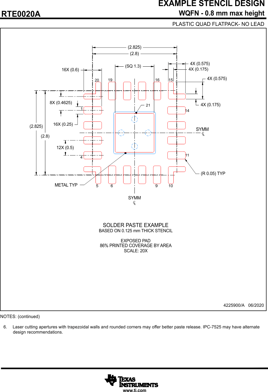
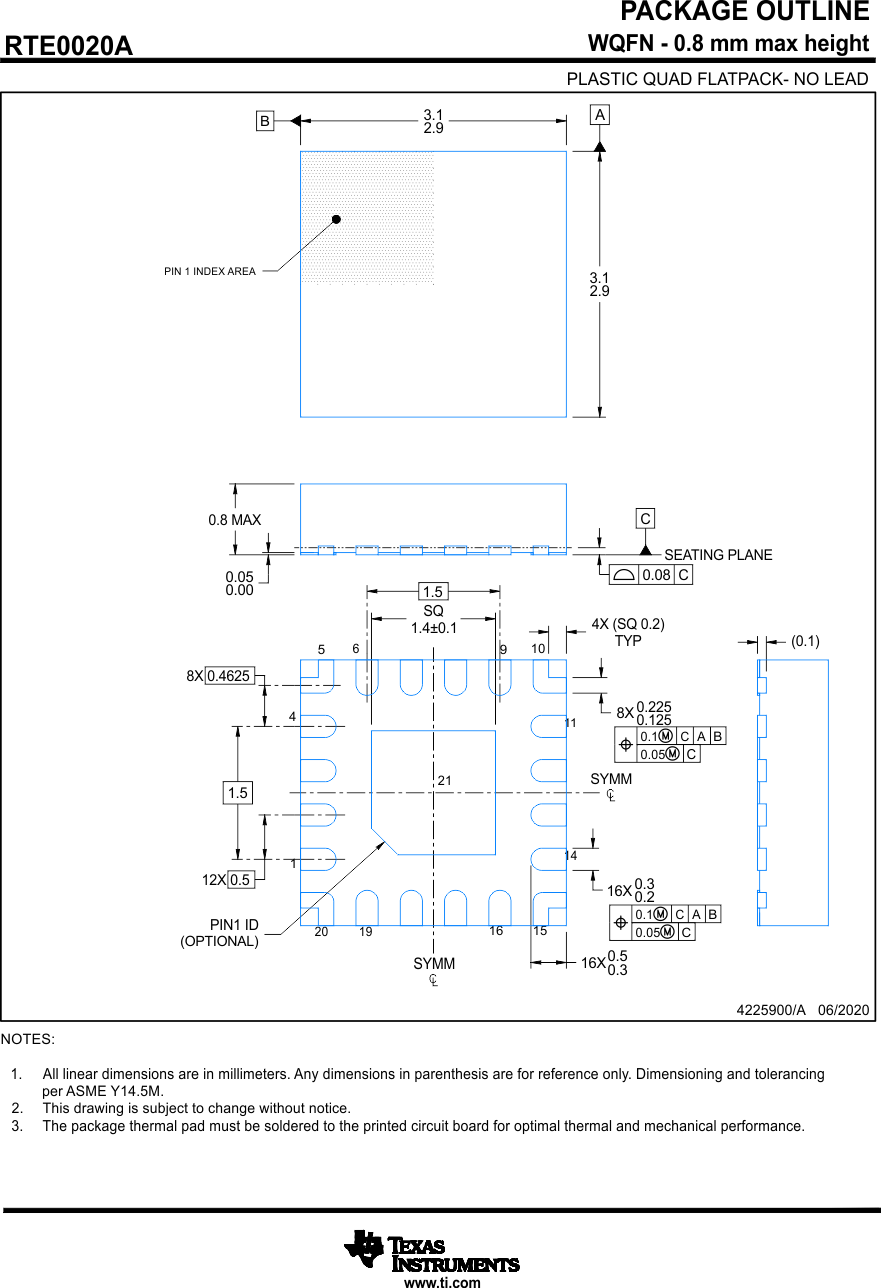
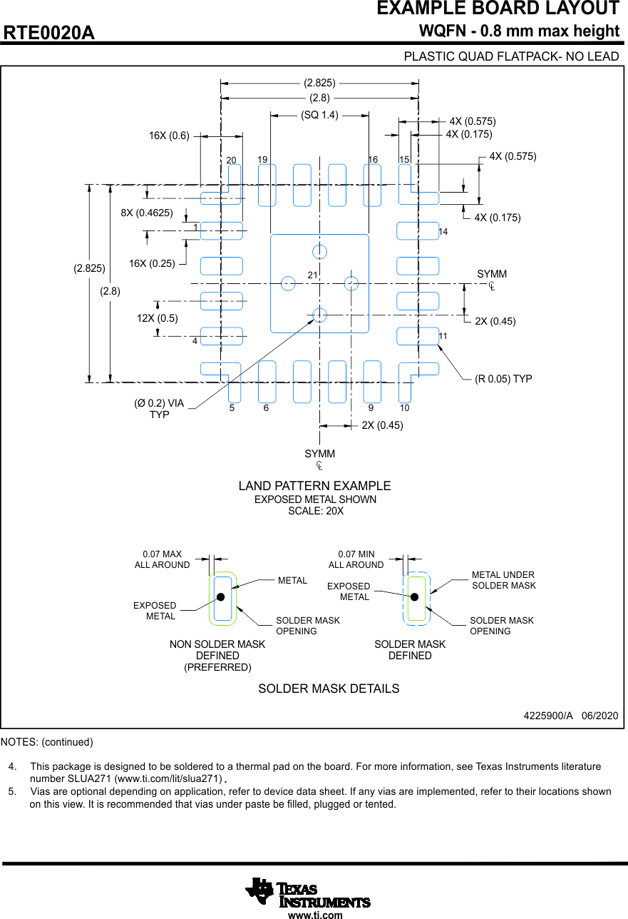
The following pages include mechanical, packaging, and orderable information. This information is the most current data available for the designated devices. This data is subject to change without notice and revision of this document. For browser-based versions of this data sheet, refer to the left-hand navigation.
GUID-20220407-SS0I-WWMX-PNV7-VQJ4FK6GLMRP-low.gif
GUID-20220407-SS0I-SC39-TGWV-WVMH47SCXMND-low.gif
GUID-20220407-SS0I-BSHL-XN7K-ZBV6TJ48G6C8-low.gif