JAJSDR1 September 2017 REF2125
PRODUCTION DATA.
9 Applications and Implementation
NOTE
Information in the following applications sections is not part of the TI component specification, and TI does not warrant its accuracy or completeness. TI’s customers are responsible for determining suitability of components for their purposes. Customers should validate and test their design implementation to confirm system functionality.
9.1 Application Information
As this device has many applications and setups, there are many situations that this datasheet can not characterize in detail. Basic applications includes positive/negative voltage reference and data acquisition systems. For more information see application sections in the REF32xx data sheet.
9.2 Typical Application: Basic Voltage Reference Connection
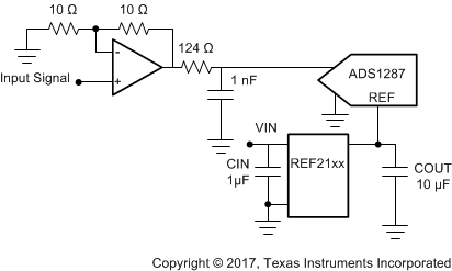
The circuit shown in Figure 28 shows the basic configuration for the REF2125 references. Connect bypass capacitors according to the guidelines in Input and Output Capacitors.
 Figure 28. Basic Reference Connection
9.2.1 Design Requirements
A detailed design procedure is described based on a design example. For this design example, use the parameters listed in Table 1 as the input parameters.
Table 1. Design Example Parameters
| DESIGN PARAMETER | VALUE |
|---|---|
| Input voltage VIN | 5 V |
| Output voltage VOUT | 2.5 V |
| REF2125 input capacitor | 1 µF |
| REF2125 output capacitor | 10 µF |
9.2.2 Detailed Design Procedure
9.2.2.1 Input and Output Capacitors
A 1-μF to 10-μF electrolytic or ceramic capacitor can be connected to the input to improve transient response in applications where the supply voltage may fluctuate. Connect an additional 0.1-μF ceramic capacitor in parallel to reduce high frequency supply noise.
A ceramic capacitor of at least 0.1 μF must be connected to the output to improve stability and help filter out high frequency noise. An additional 1-μF to 10-μF electrolytic or ceramic capacitor can be added in parallel to improve transient performance in response to sudden changes in load current; however, keep in mind that doing so increases the turnon time of the device.
Best performance and stability is attained with low-ESR, low-inductance ceramic chip-type output capacitors (X5R, X7R, or similar). If using an electrolytic capacitor on the output, place a 0.1-μF ceramic capacitor in parallel to reduce overall ESR on the output.
9.2.2.2 VIN Slew Rate Considerations
In applications with slow-rising input voltage signals, the reference exhibits overshoot or other transient anomalies that appear on the output. These phenomena also appear during shutdown as the internal circuitry loses power.
To avoid such conditions, ensure that the input voltage wave-form has both a rising and falling slew rate close to 6 V/ms.
9.2.2.3 Shutdown/Enable Feature
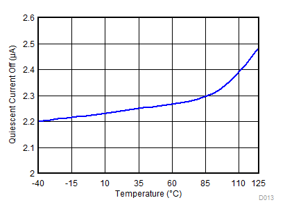
The REF2125 references can be switched to a low power shut-down mode when a voltage of 0.5 V or lower is input to the ENABLE pin. Likewise, the reference becomes operational for ENABLE voltages of 1.6 V or higher. During shutdown, the supply current drops to less than 2 μA, useful in applications that are sensitive to power consumption.
If using the shutdown feature, ensure that the ENABLE pin voltage does not fall between 0.5 V and 1.6 V because this causes a large increase in the supply current of the device and may keep the reference from starting up correctly. If not using the shutdown feature, however, the ENABLE pin can simply be tied to the IN pin, and the reference remains operational continuously.
9.2.3 Application Curves

