JAJSDR1 September 2017 REF2125
PRODUCTION DATA.
7 Parameter Measurement Information
7.1 Solder Heat Shift
The materials used in the manufacture of the REF2125 have differing coefficients of thermal expansion, resulting in stress on the device die when the part is heated. Mechanical and thermal stress on the device die can cause the output voltages to shift, degrading the initial accuracy specifications of the product. Reflow soldering is a common cause of this error.
In order to illustrate this effect, a total of 32 devices were soldered on four printed circuit boards [16 devices on each printed circuit board (PCB)] using lead-free solder paste and the paste manufacturer suggested reflow profile. The reflow profile is as shown in Figure 22. The printed circuit board is comprised of FR4 material. The board thickness is 1.65 mm and the area is 114 mm × 152 mm.
 Figure 22. Reflow Profile
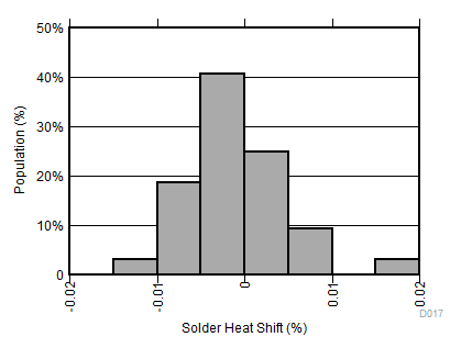
The reference and bias output voltages are measured before and after the reflow process; the typical shift is displayed in Figure 23. Although all tested units exhibit very low shifts (< 0.01%), higher shifts are also possible depending on the size, thickness, and material of the printed circuit board. An important note is that the histograms display the typical shift for exposure to a single reflow profile. Exposure to multiple reflows, as is common on PCBs with surface-mount components on both sides, causes additional shifts in the output bias voltage. If the PCB is exposed to multiple reflows, solder the device in the second pass to minimize its exposure to thermal stress.
 Figure 23. Solder Heat Shift Distribution, VREF (%)
7.2 Long-Term Stability
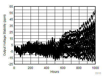
One of the key parameters of the REF2125 reference is long-term stability. Typical characteristic expressed as: curves shows the typical drift value for the REF2125 is 30 ppm from 0 to 1000 hours. This parameter is characterized by measuring 32 units at regular intervals for a period of 1000 hours. It is important to understand that long-term stability is not ensured by design and that the output from the device may shift beyond the typical 30 ppm specification at any time. For systems that require highly stable output voltages over long periods of time, the designer should consider burning in the devices prior to use to minimize the amount of output drift exhibited by the reference over time
 Figure 24. Long Term Stability - 1000 hours (VREF)
7.3 Thermal Hysteresis
Thermal hysteresis is measured with the REF2125 soldered to a PCB, similar to a real-world application. Thermal hysteresis for the device is defined as the change in output voltage after operating the device at 25°C, cycling the device through the specified temperature range, and returning to 25°C. Hysteresis can be expressed by Equation 1:

where
- VHYST = thermal hysteresis (in units of ppm)
- VNOM = the specified output voltage
- VPRE = output voltage measured at 25°C pre-temperature cycling
- VPOST = output voltage measured after the device has cycled from 25°C through the specified temperature range of –40°C to +125°C and returns to 25°C.
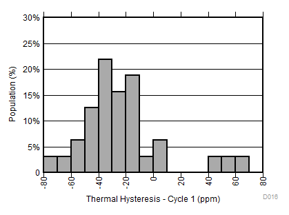
Typical thermal hysteresis distribution is as shown in Figure 25.
 Figure 25. Thermal Hysteresis Distribution (VREF)
7.4 Power Dissipation
The REF2125 voltage reference is capable of source and sink up to 10 mA of load current across the rated input voltage range. However, when used in applications subject to high ambient temperatures, the input voltage and load current must be carefully monitored to ensure that the device does not exceeded its maximum power dissipation rating. The maximum power dissipation of the device can be calculated with Equation 2:

where
- PD is the device power dissipation
- TJ is the device junction temperature
- TA is the ambient temperature
- RθJA is the package (junction-to-air) thermal resistance
Because of this relationship, acceptable load current in high temperature conditions may be less than the maximum current-sourcing capability of the device. In no case should the part be operated outside of its maximum power rating because doing so can result in premature failure or permanent damage to the device.
7.5 Noise Performance
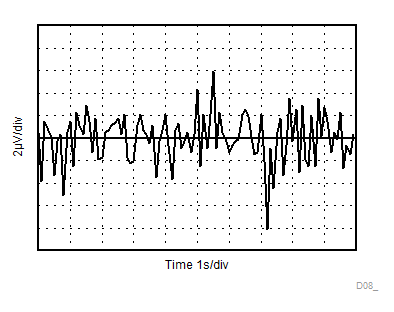
Typical 0.1-Hz to 10-Hz voltage noise can be seen in Figure 26 . Device noise increases with output voltage and operating temperature. Additional filtering can be used to improve output noise levels, although care must be taken to ensure the output impedance does not degrade ac performance. Peak-to-peak noise measurement setup is shown in Figure 26.
 Figure 26. 0.1-Hz to 10-Hz Noise (VREF)