SBVS299 April 2017
PRODUCTION DATA.
- 1 Features
- 2 Applications
- 3 Description
- 4 Revision History
- 5 Device Comparison Table
- 6 Pin Configuration and Functions
- 7 Specifications
- 8 Detailed Description
- 9 Application and Implementation
- 10Power Supply Recommendations
- 11Layout
- 12Device and Documentation Support
- 13Mechanical, Packaging, and Orderable Information
8 Detailed Description
8.1 Overview
The REF31xx-Q1 is a family of series, CMOS, precision bandgap voltage references. The basic bandgap topology is shown in Functional Block Diagram. Transistors Q1 and Q2 are biased such that the current density of Q1 is greater than that of Q2. The difference of the two base-emitter voltages, Vbe1 – Vbe2, has a positive temperature coefficient and is forced across resistor R1. This voltage is gained up and added to the base-emitter voltage of Q2, which has a negative temperature coefficient. The resulting output voltage is virtually independent of temperature. The curvature of the bandgap voltage, as shown in Figure 3, is due to the slightly nonlinear temperature coefficient of the base-emitter voltage of Q2.
8.2 Functional Block Diagram

8.3 Feature Description
8.3.1 Supply Voltage
The REF31xx-Q1 family of references features an extremely low dropout voltage. With the exception of the REF3112, which has a minimum supply requirement of 1.8 V, these references can be operated with a supply of only 5 mV above the output voltage in an unloaded condition. For loaded conditions, a typical dropout voltage versus load is shown in Typical Characteristics.
The REF31xx-Q1 features a low quiescent current that is extremely stable over changes in both temperature and supply. The typical room temperature quiescent current is 100 μA, and the maximum quiescent current over temperature is just 135 μA. The quiescent current typically changes less than 2 μA over the entire supply range, as shown in Figure 20.
 Figure 20. Supply Current vs Supply Voltage
Supply voltages below the specified levels can cause the REF31xx-Q1 to momentarily draw currents greater than the typical quiescent current. This can be prevented by using a power supply with a fast rising edge and low output impedance.
8.3.2 Thermal Hysteresis
Thermal hysteresis for the REF31xx-Q1 is defined as the change in output voltage after operating the device at 25°C, cycling the device through the specified temperature range, and returning to 25°C. It can be expressed as:

where
8.3.3 Temperature Drift
The REF31xx-Q1 is designed to exhibit minimal drift error, defined as the change in output voltage over varying temperature. The drift is calculated using the box method, which is described in Equation 2:

The REF31xx-Q1 features a typical drift coefficient of 5 ppm from 0°C to 70°C, the primary temperature range for many applications. For the industrial temperature range of –40°C to +125°C, the REF31xx-Q1 family drift increases to a typical value of 10 ppm.
8.3.4 Noise Performance
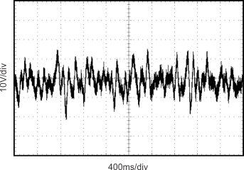
Typical 0.1-Hz to 10-Hz voltage noise can be seen in Figure 21. The noise voltage of the REF31xx-Q1 increases with output voltage and operating temperature. Additional filtering may be used to improve output noise levels, although take care to ensure the output impedance does not degrade the AC performance.
 Figure 21. 0.1-Hz to 10-Hz Noise
8.3.5 Long-Term Stability
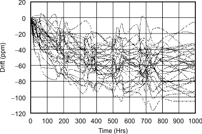
Long-term stability refers to the change of the output voltage of a reference over a period of months or years. This effect lessens as time progresses, as is shown by the long-term stability curves. The typical drift value for the REF31xx-Q1 is 70 ppm from 0 to 1000 hours. This parameter is characterized by measuring 30 units at regular intervals for a period of 1000 hours.
 Figure 22. REF3112 Long-Term Stability
8.3.6 Load Regulation
Load regulation is defined as the change in output voltage due to changes in load current. The load regulation of the REF31xx-Q1 is measured using force and sense contacts as pictured in Figure 23. The force and sense lines reduce the impact of contact and trace resistance, resulting in accurate measurement of the load regulation contributed solely by the REF31xx-Q1. For applications requiring improved load regulation, force and sense lines must be used.
 Figure 23. Accurate Load Regulation of REF31xx-Q1
8.4 Device Functional Modes
8.4.1 Negative Reference Voltage
For applications requiring a negative and positive reference voltage, the REF31xx-Q1 and OPA703 can be used to provide a dual-supply reference from a ±5-V supply. Figure 24 shows the REF3125-Q1 used to provide a ±2.5-V supply reference voltage. The low drift performance of the REF31xx-Q1 complements the low offset voltage and low drift of the OPA703 to provide an accurate solution for split-supply applications.
 Figure 24. REF3125-Q1 Combined With OPA703 to Create Positive and Negative Reference Voltages
8.4.2 Data Acquisition
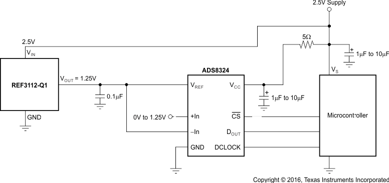
Data acquisition systems often require stable voltage references to maintain accuracy. The REF31xx-Q1 family features stability and a wide range of voltages suitable for most microcontrollers and data converters. Figure 25, Figure 26, and Figure 27 show basic data acquisition systems.
 Figure 25. Basic Data Acquisition System 1
 Figure 26. Basic Data Acquisition System 2
 Figure 27. REF3140-Q1 Provides an Accurate Reference for Driving the ADS8381