SBOS471B April 2010 – June 2015 REF5020-EP , REF5025-EP , REF5040-EP , REF5050-EP
PRODUCTION DATA.
- 1 Features
- 2 Applications
- 3 Description
- 4 Revision History
- 5 Pin Configuration and Functions
- 6 Specifications
- 7 Detailed Description
- 8 Application and Implementation
- 9 Power Supply Recommendations
- 10Layout
- 11Device and Documentation Support
- 12Mechanical, Packaging, and Orderable Information
8 Application and Implementation
NOTE
Information in the following applications sections is not part of the TI component specification, and TI does not warrant its accuracy or completeness. TI’s customers are responsible for determining suitability of components for their purposes. Customers should validate and test their design implementation to confirm system functionality.
8.1 Application Information
The REF50xx devices are low-noise, precision bandgap voltage references that are specifically designed for excellent initial voltage accuracy and drift. View the Functional Block Diagram of the REF50xx.
When designing circuits with a voltage reference, output noise is one of the main concerns. The main source of voltage noise in the reference voltages originates from the bandgap and output amplifier, which contribute significantly to the overall noise. During the design process, it is important to minimize these sources of voltage noise.
8.2 Typical Applications
8.2.1 Negative Reference Voltage
For applications requiring a negative and positive reference voltage, the REF50xx and OPA735 can be used to provide a dual-supply reference from a 5-V supply. Figure 25 shows the REF5020 used to provide a 2.5-V supply reference voltage. The low-drift performance of the REF50xx complements the low offset voltage and zero drift of the OPA735 to provide an accurate solution for split-supply applications. Care must be taken to match the temperature coefficients of R1 and R2.
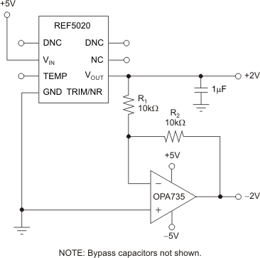 Figure 25. The REF5020 and OPA735 Create Positive and Negative Reference Voltages
8.2.1.1 Design Requirements
When using REF50xx in the design, it is important to select proper capacitive load that will not create gain peaking adding noise to the output voltage. At the same time, the capacitor must be selected to provide required filtering performance for the system. In addition, input bypass capacitor and noise reduction capacitors must be added for optimum performances.
8.2.1.2 Detailed Design Procedure
Proper design procedure will require first to select output capacitor. If the ESR of the capacitor is not in 1-Ω range additional resistor must be added in series with the load capacitor. Next, add a 1-µF capacitor to the NR pin to reduce internal noise of the REF50xx. Measuring output noise will confirm if the design has met the initial target.
8.2.2 Positive Reference Voltage
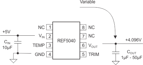 Figure 28. REF50xx With Load Capacitor
8.2.2.1 Detailed Design Procedure
8.2.2.1.1 Load Capacitance
To determine how much noise the reference voltage is contributing in a real application, this design uses the circuit presented in Figure 28. For the same conditions as power supply, input decoupling, and load current, measure the output noise for different output decoupling or load capacitors. The load capacitor type will change the low-pass filter frequency that is created on the output. This filter is determined by an added capacitor value and two parasitic components: the open-loop output impedance of the internal amplifier to the reference voltage, and the ESR of the external capacitor.
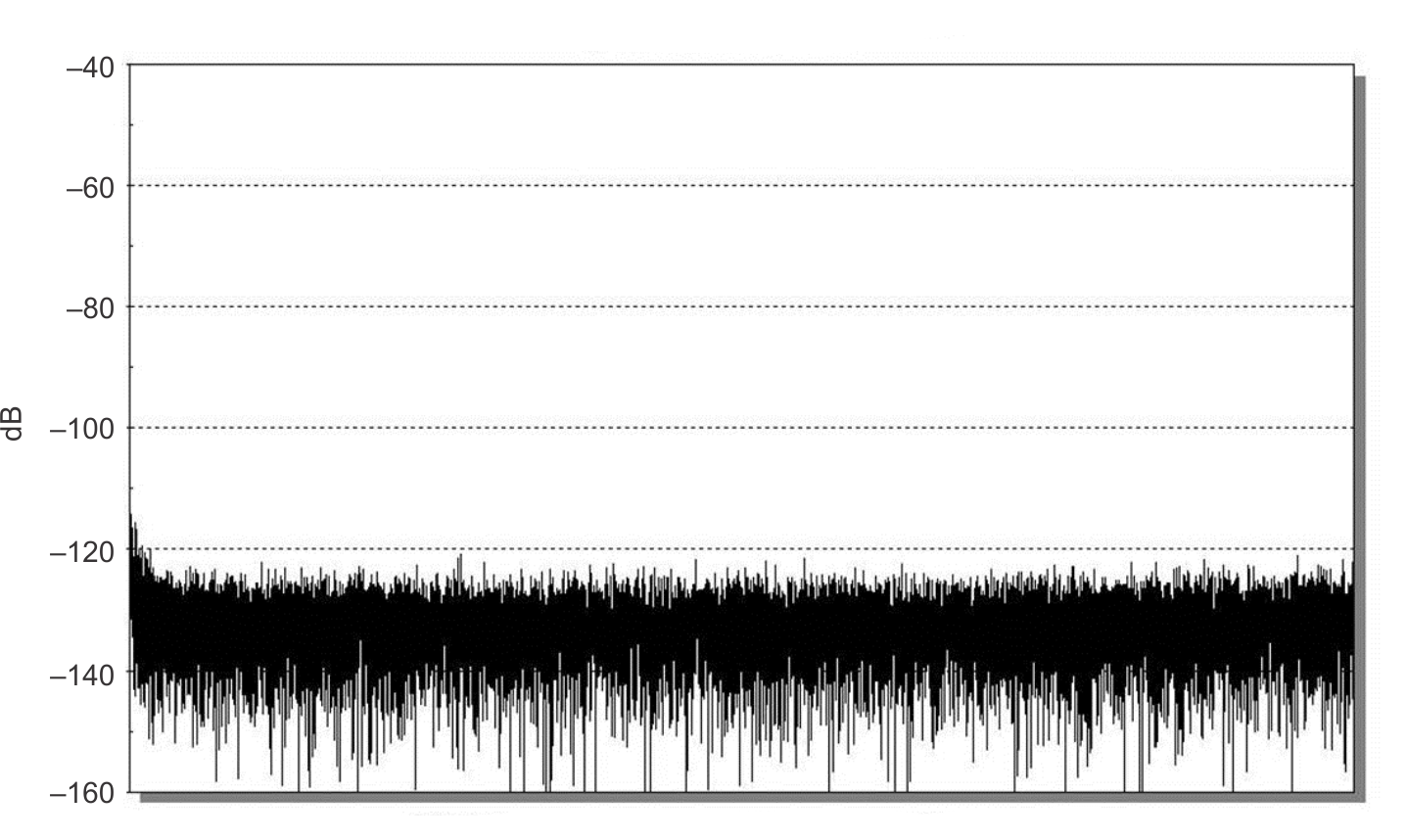
Figure 29 shows a fast-Fourier-transform (FFT) plot of the output signal of the reference voltage circuit with a 10-μF ceramic capacitor load. The output noise level peaks at around 9 kHz because of the response of the internal amplifier of the circuit to the capacitive load (CL).
This peaking is the main contributor to the overall measured noise. This output noise, measured with an analog meter over a frequency range of up to 80 kHz, is approximately 16.5 μVRMS. If the voltage-reference circuit was connected to the input of an ADC, the measured noise across a 65-kHz frequency range would be 138 μVPP. This noise level makes this solution adequate for 8- to 14-bit converters.
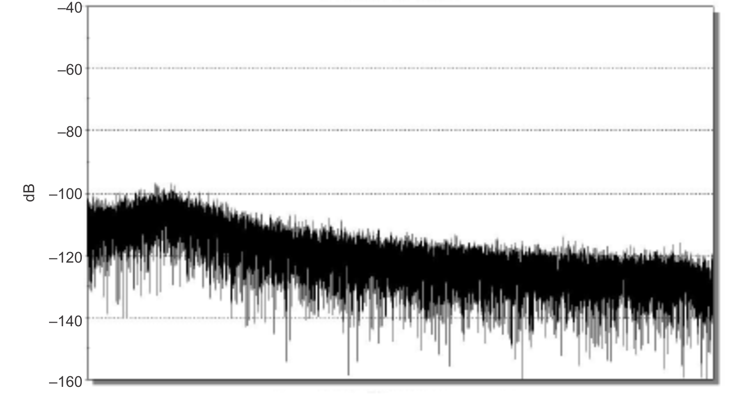 Figure 29. REF50xx FFT Plot of the Noise
 With 10-µF Load Capacitor and 10-µΩ ESR
Every capacitor can be represented with a complicated equivalent model, which is voltage and frequency dependent with a large number of passive components. For the purposes of this design, this model is limited to the few components. The biggest impact on the creation of the low-pass filter and stability analysis is the simplified model of equivalent series inductance and resistance. Considering good layout practice and inherently low equivalent series inductance of today’s components, this model in the future analysis will be presented only by equivalent capacitance and series resistance.
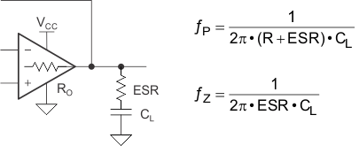 Figure 30. Equivalent SCH Of REF50xx With Load Capacitor for Stability Analysis
When evaluating the impact of ESR and CL on the performance the reference voltage, it is important to include the effect of the open-loop output resistance (RO) of the output amplifier. The combination of RO, ESR, and CL modifies the open-loop response curve by introducing one pole (fP) and one zero (fZ). The values RO, ESR, and CL determine the corner frequency of the added pole fP; and the values of ESR and CL determine the corner frequency of the added zero.
The introduction of the external ESR-CL on the output of the reference voltage modifies the output amplifier open-loop gain curve. The added pole modifies the open-loop gain curve of the reference voltage output amplifier by introducing a –20 dB/decade change at the frequency fP to the already –20 dB/decade slope of the open-loop gain curve, making the slope equal to –40 dB/decade. The added zero at frequency fZ changes the open-loop gain curve back to –20 dB/decade.
Table 1. Noise Measurement Results for Different Load Capacitors
| NOISE | 22 kHz LP-5P |
30 kHz LP-3P |
80 kHz LP-3P |
>500 kHz | UNIT |
|---|---|---|---|---|---|
| GND | 0.8 | 1 | 1.8 | 4.9 | µVRMS |
| 1 µF | 37.8 | 41.7 | 53.7 | 9,017 | |
| 2.2 µF (cer) | 41.7 | 46.2 | 55.1 | 60.8 | |
| 10 µF | 33.4 | 33.4 | 35.2 | 38.5 | |
| 10 µF (cer) | 37.1 | 37.2 | 37.8 | 39.1 | |
| 20 µF (cer) | 33.1 | 33.1 | 33.2 | 34.5 | |
| 47 µF | 23.2 | 23.8 | 24.1 | 26.5 |
Table 1 shows the measured noise values for different frequency bandwidths as well as different values and types of external capacitors. These measurements show that low-ESR (approximately 100-mΩ) ceramic capacitors tend to increase the noise, compared to normal-ESR (approximately 2-Ω) tantalum capacitors. This tendency is caused by a stability issue with the output amplifier and gain peaking in the amplifier frequency response.
8.2.2.1.2 Bandgap Noise Reduction
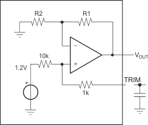 Figure 31. REF50xx Internal Structure of Trim/NR Pin
The internal schematic of the REF50xx device shows that the trim pin allows direct access to the bandgap output. Figure 31 shows the trim pin connection to the internal bandgap circuit through a resistor. Adding a capacitor on the trim pin creates a lowpass filter that has a broadband attenuation of −21 dB.
For example, a small 1-μF capacitor adds a pole at 14.5 Hz and a zero at 160 Hz. If more filtering is needed, a larger value capacitor can be added, which will lower the filter cutoff frequency and the noise contributed by the bandgap.
Table 2. Measured Noise (µVRMS) for Four Bandwidths
| NOISE | 22 kHz (LOW-PASS 5-POLE) | 30 kHz (LOW-PASS 3-POLE) | 80 kHz (LOW-PASS 3-POLE) | > 500 kHz | UNIT |
|---|---|---|---|---|---|
| GND | 0.8 | 1 | 1.8 | 4.6 | µVRMS |
| 2.2 µF (ceramic) | 42.5 | 47.2 | 61.2 | 68.3 | |
| 2.2 µF + 1 µF | 17.5 | 19.4 | 22.6 | 24.5 | |
| 10 µF (ceramic) | 34.4 | 35.6 | 37.7 | 44.5 | |
| 10 µF + 1 µF | 14.1 | 14.4 | 14.9 | 16.4 | |
| 20 µF (ceramic) | 34.8 | 34.9 | 35.1 | 35.2 | |
| 20 µF + 1 µF | 14.4 | 14.4 | 14.7 | 15.1 |
Adding a 1-μF capacitor in this example filters the noise contribution of the bandgap and lowers the total noise by a factor of 2.5 times.
8.3 System Example
8.3.1 Data Acquisition
Data acquisition systems often require stable voltage references to maintain accuracy. The REF50xx family features low noise, very low drift, and high initial accuracy for high-performance data converters. Figure 32 shows the REF5040 in a basic data acquisition system.
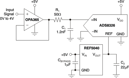 Figure 32. Basic Data Acquisition System
During the design of the data acquisition system, equal consideration must be given to the buffering analog input signal as well as the reference voltage. Having a properly designed input buffer with an associated RC filter is a necessary requirement, but does not ensure the maximum performance.
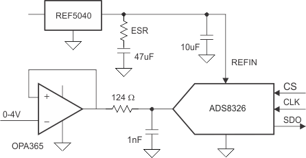 Figure 33. Complete Data Acquisition System Using REF50xx
Three measurements using different components of the output are shown for this data acquisition system.
Table 3. Data Acquisition Measurement Results for Different Conditions
| OPA365 | 124 Ω, 1 nF | 124 Ω, 1 nF | 124 Ω, 100 µF | |
|---|---|---|---|---|
| REF5040 | 10 µF | 10 µF + 47 µF | 10 µF + 47 µF | UNIT |
| TRIM | 0 µF | 1 µF | 1 µF | |
| Resolution | 16 | 16 | 16 | Bits |
| States | 65536 | 65536 | 65536 | |
| VREF | 4.096 | 4.096 | 4.096 | V |
| LSB | 62.5 | 62.5 | 62.5 | µV |
| VIN | 4.02 | 4.02 | 4.02 | V |
| Data Std | 1.07 | 0.53 | 0.41 | LSB |
| Noise | 67.0 | 33.4 | 25.8 | µVRMS |
| Noise | 442.3 | 220.5 | 170.2 | µVPP |
| SNR | 86.7 | 92.8 | 95.0 | dB |
| FTT Points | 32768 | 32768 | 32768 | |
| Noise Flor | –128.8 | –134.9 | –131.7 | dB |
Once the correct components for data acquisition system from Figure 33 are selected, measurement results can be compared to the ADS8326 data sheet specifications.
Table 4. AC Performance for Data Acquisition System from Figure 33
| ADS8326 | ADS8326B | SYSTEM | SYSTEM | ||
|---|---|---|---|---|---|
| REF5040 | DATA SHEET | DATA SHEET | LOW ESR | 10 µF + 47 µF | UNIT |
| TRIM | 1µF | ||||
| SNR | 91 | 91.5 | 90.6 | 92.2 | dB |
| SINAD | 87.5 | 88 | 85.7 | 89.5 | dB |
| SFDR | 94 | 95 | 88.3 | 98.4 | dB |
| THD | –90 | –91 | –87.3 | –92.9 | dB |
| ENOB | 14.28 | 14.35 | 13.94 | 14.58 | Bits |
Table 3 shows improvements on the FFT for a properly designed system.
