JAJSC87B May 2016 – August 2016 REF6125 , REF6130 , REF6133 , REF6141 , REF6145 , REF6150
PRODUCTION DATA.
8 Parameter Measurement Information
8.1 Solder Heat Shift
The materials used in the manufacture of the REF61xx have differing coefficients of thermal expansion, and result in stress on the device die when the part is heated. Mechanical and thermal stress on the device die sometimes causes the output voltages to shift, degrading the initial accuracy specifications of the product. Reflow soldering is a common cause of this error.
In order to illustrate this effect, a total of 128 devices were soldered on eight printed circuit boards (PCBs), with 16 devices on each PCB, using lead-free solder paste, and the manufacturer-suggested reflow profile. The reflow profile is as shown in Figure 40. The printed circuit board is comprised of FR4 material. The board thickness is 1.65 mm and the area is 101.6 mm × 127 mm.
The reference output voltage is measured before and after the reflow process; the typical shift is displayed in Figure 41. Although all tested units exhibit very low shifts (< 0.03%), higher shifts are also possible depending on the size, thickness, and material of the PCB.
The histogram displays the typical shift for exposure to a single reflow profile. Exposure to multiple reflows, as is common on PCBs with surface-mount components on both sides, causes additional shifts in the output bias voltage. If the PCB is exposed to multiple reflows, solder the device in the final pass to minimize exposure to thermal stress.
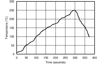 Figure 40. Reflow Profile
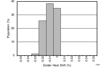 Figure 41. Solder Heat Shift Distribution
8.2 Thermal Hysteresis
Thermal hysteresis for the device is defined as the change in output voltage after operating the device at 25°C, cycling the device through the specified temperature range, and returning to 25°C. Thermal hysteresis was measured with the REF61xx soldered to a PCB, similar to a real-world application. The PCB was baked at 150°C for 30 minutes before thermal hysteresis was measured. Thermal hysteresis is expressed as:

where
- VHYST = thermal hysteresis (in units of ppm).
- VNOM = the specified output voltage.
- VPRE = output voltage measured at 25°C pretemperature cycling.
- VPOST = output voltage measured after the device has cycled from 25°C through the specified temperature range of –40°C to 125°C and returns to 25°C.
Typical thermal hysteresis distribution is shown in Figure 42 and Figure 43.
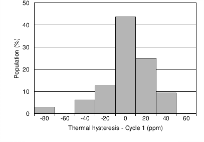 Figure 42. Thermal Hysteresis Distribution (Cycle 1)
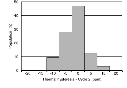 Figure 43. Thermal Hysteresis Distribution (Cycle 2)
8.3 Reference Droop Measurements
Many applications, such as event-triggered and multiplexed data-acquisition systems, require the very first conversion of the ADC to have 18-bit or greater precision. These types of data-acquisition systems capture data in bursts, and are also called burst-mode, data-acquisition systems. Achieving 18-bit precision for the first sample is a very difficult using a conventional voltage reference because the voltage reference droop limits the accuracy of the first few conversions. The REF61xx have an integrated ADC drive buffer that makes sure the reference droop is less than 1 LSB at 18-bit precision when used with the ADS8881, even at full throughput. Figure 44 and Figure 45 show the REF61xx output voltage droop when driving the REF pin of the ADS8881 at positive and negative full-scale inputs, respectively.
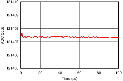
| REF6150 driving REF pin of ADS8881 operating at 1 MSPS, | ||
| positive full-scale input to ADS8881 |
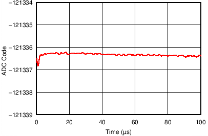
| REF6150 driving REF pin of ADS8881 operating at 1 MSPS, | ||
| negative full-scale input to ADS8881 |
Direct measurement of the reference droop to 18-bit accuracy can be a challenging process. Therefore, the plots in Figure 44 and Figure 45 were obtained by processing the output code of the ADC. The ADC output code is given by:
If the input voltage is kept constant, VREF is computed by monitoring the ADC output code C. The ADC code usually has six to seven LSBs of code spread due to the inherent noise of the ADC. In order to measure reference droop, this noise must be reduced drastically. Noise reduction is done by averaging the output code multiple times, as described in the next paragraph.
Figure 46 shows the setup that was used to measure the reference droop. The output ADC code was captured using a field-programmable gate array (FPGA), and post-processing was done on a personal computer. The input to the THS4521, and hence in turn to the ADS8881, is a constant dc voltage (close to positive or negative full-scale because this condition is the worst-case for charge drawn from the REF pin). The dc source must have extremely low noise. After the REF61xx device is powered up and stable, the FPGA sends commands to the ADS8881 to capture data in bursts. The ADS8881 is initially in idle mode for 100 ms. The FPGA then sends a command to the ADS8881 to perform 100 conversions at 1 MSPS. The ADC code corresponding to these 100 conversions (one burst of data) is stored as the first row in a 1000 × 100 dimensional array. This operation is repeated 1000 times, and the data corresponding to each burst is stored in a new row of the 1000 × 100 dimensional array. Finally, each column in this array is averaged to get a final data-set of 100 elements. This final data-set now has code spread that is much less than 1 LSB because most of the noise has now been removed through averaging. This data-set was plotted on a graph with X axis = column number (each column number corresponds to 1 µs of time because the sampling rate is 1 MSPS), and Y axis = ADC output code to obtain reference-droop measurements.
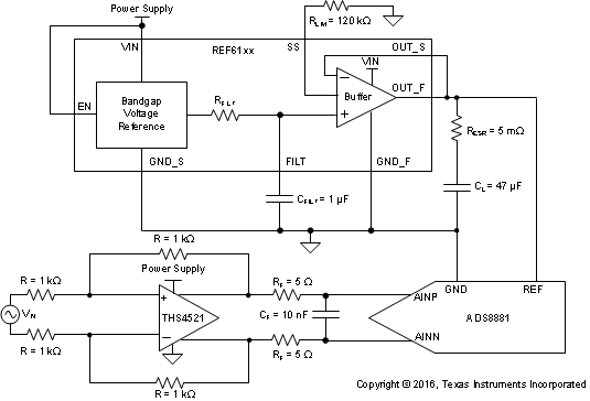 Figure 46. Burst-Mode Measurement Setup
8.4 1/f Noise Performance
Typical 0.1-Hz to 10-Hz voltage noise for the REF6125 is shown in Figure 47. The 1/f noise scales with output voltage, but remains 3 µVPP/V for all the variants. Peak-to-peak noise measurement setup is shown in Figure 48.
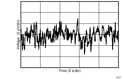 Figure 47. 0.1-Hz to 10-Hz Noise
 Figure 48. 0.1-Hz to 10-Hz Noise Measurement Setup