JAJSC87B May 2016 – August 2016 REF6125 , REF6130 , REF6133 , REF6141 , REF6145 , REF6150
PRODUCTION DATA.
10 Applications and Implementation
NOTE
Information in the following applications sections is not part of the TI component specification, and TI does not warrant its accuracy or completeness. TI’s customers are responsible for determining suitability of components for their purposes. Customers should validate and test their design implementation to confirm system functionality.
10.1 Application Information
Many applications, such as event-triggered and multiplexed data-acquisition systems, require the very first conversion of the ADC to have 18-bit or greater precision. These types of data acquisition systems capture data in bursts, and are also called burst-mode, data-acquisition systems. Achieving 18-bit precision for the first sample is very difficult using a conventional voltage reference because the voltage reference droop limits the accuracy of the first few conversions. Furthermore, variable-sampling-rate systems require that the gain error of the system does not vary with sampling rate. The primary objective of this design example is to demonstrate the lowest distortion and noise, burst-mode data-acquisition block with low power consumption, using an 18-bit SAR ADC operating at a throughput of 1 MSPS, for a 1-kHz, full-scale, pure sine-wave input.
10.2 Typical Application
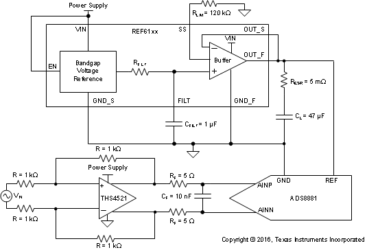 Figure 54. 18-bit, 1-MSPS, Burst-Mode Data Acquisition system
10.2.1 Design Requirements
- Burst-mode support (see Reference Droop Measurements section for more details)
- ENOB > 16 bits
- THD < –120 dB
- Power consumption < 50 mW
- Throughput = 1 MSPS
10.2.2 Detailed Design Procedure
The data acquisition system shown in Figure 54 has three major contributors to the noise and accuracy in the system: the input driver, the reference with driver, and the data converter. Each analog block is carefully designed so that the data converter specifications limit the system specifications. The THS4551, a fully differential operational amplifier is used to drive the 18-bit ADC (ADS8881). The charge-kickback RC filter at the output of the THS4551 is used to reduce the charge kickback created by the opening and closing of the sampling switch inside the ADC. Design the RC filter so that the voltage at the sampling capacitor settles to 18-bit accuracy within the acquisition time of the ADC.
Data-acquisition systems require stable and accurate voltage references in order to perform the most accurate data conversion. The REF61xx family of voltage references have integrated an ADC drive buffer, and can therefore drive the REF pin of the ADS8881 directly, without the need for an external reference buffer. See the Integrated ADC Drive Buffer section for more details about reference-buffer requirements. Correct output capacitor selection for the REF61xx is very important in this design. The Stability section describes the ESR requirements of the output capacitor for stability and burst-mode requirements. A capacitance of 1 μF is connected to the FILT pin to reduce broadband noise of the REF61xx.
10.2.2.1 Results
Table 1 summarizes the measured results.
Table 1. Measured Results
| SPECIFICATION | MEASURED RESULT |
|---|---|
| SNR | 100.5 dB |
| ENOB | 16.4 |
| THD | –125.9 dB |
| Throughput | 1 MSPS |
| Burst mode | First sample > 18-bit precision |
| Power consumption | 40 mW |
10.2.3 Application Curves
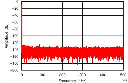
| REF6150 driving REF pin of ADS8881, | ||
| fIN = 1 kHz, SNR = 100.5 dB, THD = –125.9 dB |
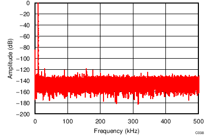
| REF6150 driving REF pin of ADS8881, | ||
| fIN = 10 kHz, SNR = 99.2 dB, THD = –119.4 dB |
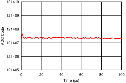
| REF6150 driving REF pin of ADS8881 operating at 1 MSPS, | ||
| positive full-scale input to ADS8881 |
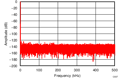
| REF6150 driving REF pin of ADS8881, | ||
| fIN = 2 kHz, SNR = 100.4 dB, THD = –123.9 dB |
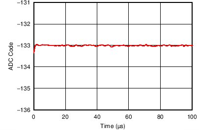
| REF6150 driving REF pin of ADS8881 operating at 1 MSPS, | ||
| AINP = AINN = VREF / 2 for ADS8881 |
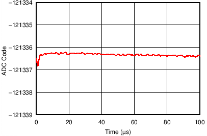
| REF6150 driving REF pin of ADS8881 operating at 1 MSPS, | ||
| negative full-scale input to ADS8881 |